
Embedded RFID tag packaging method

A technology of RFID tags and packaging methods, applied to record carriers, instruments, electrical components, etc. used in machines, can solve problems such as low matching, poor thermal-mechanical properties of labels, poor thermal-mechanical properties, etc., to achieve anti-vibration performance and The effect of improved bending resistance, improved thermomechanical properties, and improved hygroscopic properties

Inactive Publication Date: 2019-12-13
BEIJING SMARTCHIP MICROELECTRONICS TECH COMPANY +2
View PDF3 Cites 1 Cited by
  • Summary
  • Abstract
  • Description
  • Claims
  • Application Information

AI Technical Summary

Problems solved by technology

COB packaged RFID tags have the advantages of simple manufacturing process and low cost, but due to the low matching degree of thermal expansion coefficient (Coefficient of Thermal Expansion, CTE) of vinyl, PCB board and RFID chip, resulting in poor thermomechanical properties; and The hygroscopicity and manufacturability of black glue are very low, which also directly affects the reliability of COB packaged RFID tags
SMT module RFID packaging can meet high reliability requirements, but SMT module packaging RFID tags must go through the reflow process (220-260 ° C) to form solder joints to realize the interconnection between the RFID module pins and the antenna. During the reflow process due to moisture- Thermal-mechanical stress coupling is very prone to "popcorn effect", which affects packaging yield and reliability; and SMT module packaging RFID cannot meet the development needs of light, thin and small
For the COB and SMT module packaging methods of RFID tags, the CTE matching is not very good, resulting in poor thermal-mechanical properties of the tag, and the deformation of the tag due to temperature changes, which affects the sensitivity and reliability of the RFID tag.

Method used


Image

  • Embedded RFID tag packaging method
  • Embedded RFID tag packaging method
  • Embedded RFID tag packaging method

Examples


Embodiment Construction

[0026] The specific embodiments of the present invention will be described in detail below in conjunction with the accompanying drawings, but it should be understood that the protection scope of the present invention is not limited by the specific embodiments.

[0027] Unless expressly stated otherwise, throughout the specification and claims, the term "comprise" or variations thereof such as "includes" or "includes" and the like will be understood to include the stated elements or constituents, and not Other elements or other components are not excluded.

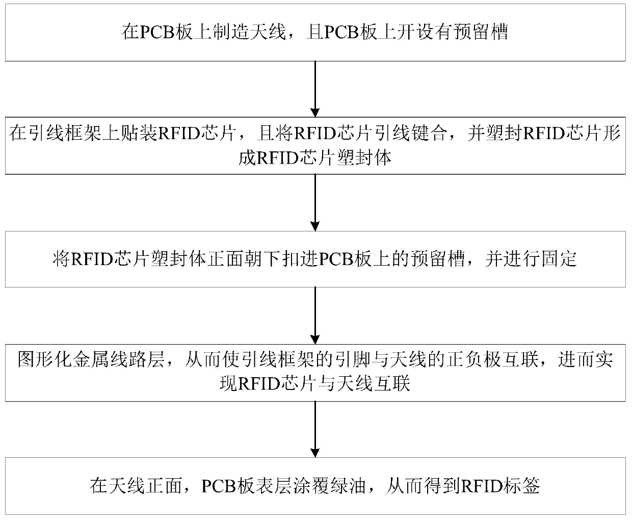
[0028] Such as Figure 1 to Figure 10 as shown, figure 1 It is a flow chart of steps of an embedded RFID tag packaging method according to an embodiment of the present invention; figure 2 It is a schematic diagram of the process of opening a reserved slot on a PCB board according to an embedded RFID tag packaging method according to an embodiment of the present invention; image 3 It is a schematic diagram of the proces...


PUM


Abstract

The invention discloses an embedded RFID tag packaging method, which comprises the steps of manufacturing an antenna on a PCB, and forming a reserved groove in the PCB; mounting an RFID chip on a leadframe, performing lead bonding on the RFID chip, and plastically packaging the RFID chip to form an RFID chip plastic package body; buckling the RFID chip plastic package body into the reserved groove in the PCB in a mode of enabling the front of the RFID chip plastic package body to face downwards, and fixing the RFID chip plastic package body; patterning a metal circuit layer, enabling pins ofthe lead frame to be interconnected with the positive electrode and the negative electrode of the antenna, and thus realizing the interconnection between the RFID chip and the antenna; and coating thefront of the antenna and the surface layer of the PCB with green oil to obtain an RFID tag. Therefore, the embedded RFID tag packaging method provided by the invention can meet the requirement of thin and high-reliability packaging.

Description

technical field [0001] The invention relates to the technical field of RFID hard tag manufacturing, in particular to an embedded RFID tag packaging method. Background technique [0002] The Internet of Things is to connect any item to the Internet according to an agreed agreement through information sensing equipment such as two-dimensional code reading equipment, radio frequency identification (RFID) devices, infrared sensors, global positioning systems, and laser scanners. A network that exchanges and communicates to realize intelligent identification, positioning, tracking, monitoring and management. In recent years, with the rapid development of the Internet of Things, the RFID tag industry has developed rapidly. Currently, RFID tag packaging mainly includes three packaging methods: COB (Chip On Board) packaging, FC (Flip Chip) packaging and SMT (Surface Mount Technology) module packaging. [0003] For special-shaped labels with plastic shells, there are mainly two meth...

Claims


Application Information

Patent Timeline
Patent Type & Authority Applications(China)
IPC IPC(8): H01L21/56H01L23/31H01L23/66G06K19/077
CPCG06K19/07718G06K19/07728H01L21/56H01L23/3107H01L23/66H01L2223/6677H01L2224/48091H01L2224/73265H01L2924/181H01L2924/00012H01L2924/00014
Inventor 韩顺枫唐晓柯李德建关媛李博夫
Owner BEIJING SMARTCHIP MICROELECTRONICS TECH COMPANY
Learn More