Semiconductor device, manufacturing method and mask

A manufacturing method and semiconductor technology, which are applied to semiconductor devices, electrical solid-state devices, electrical components, etc., can solve the problems of poor uniformity of key dimensions of word lines, etching load effects, abnormal contours and depths, etc. Erosion loading effect, improved device performance, improved uniformity

Active Publication Date: 2021-09-03
SEMICON MFG INT (SHANGHAI) CORP +1
View PDF3 Cites 0 Cited by
  • Summary
  • Abstract
  • Description
  • Claims
  • Application Information

AI Technical Summary

Problems solved by technology

[0004] In practice, it has been found that when the gates of the dense region and the sparse region are formed in the same etching process, there is an etching difference (I / D loading, or called sparse / dense loading effect), affected by the I / D loading, the gates at the edge of the dense area tend to have abnormal contours and depths, and the abnormal edge gates will affect the middle of the dense area. Both the gate and the gate of the sparse region are adversely affected, which in turn affects the performance of the device
For example, in a NAND flash memory, the distribution density of the select gate (select gate, SG, that is, a sparse gate) and the word line (wordline, WL, corresponding to a control gate, that is, a dense gate) are different, and the select gate The distance between its nearest neighbor word line is greater than the distance between two adjacent word lines. As the critical size of NAND flash memory shrinks day by day, there will be increasingly serious etching load between word line and select gate. effect, which makes the CD uniformity of the word line worse, and multiple word lines on the edge (that is, multiple word lines close to the select gate) often produce abnormalities in profile and depth, which in turn affects the performance of the device

Method used


Image

  • Semiconductor device, manufacturing method and mask
  • Semiconductor device, manufacturing method and mask
  • Semiconductor device, manufacturing method and mask

Examples


Embodiment Construction

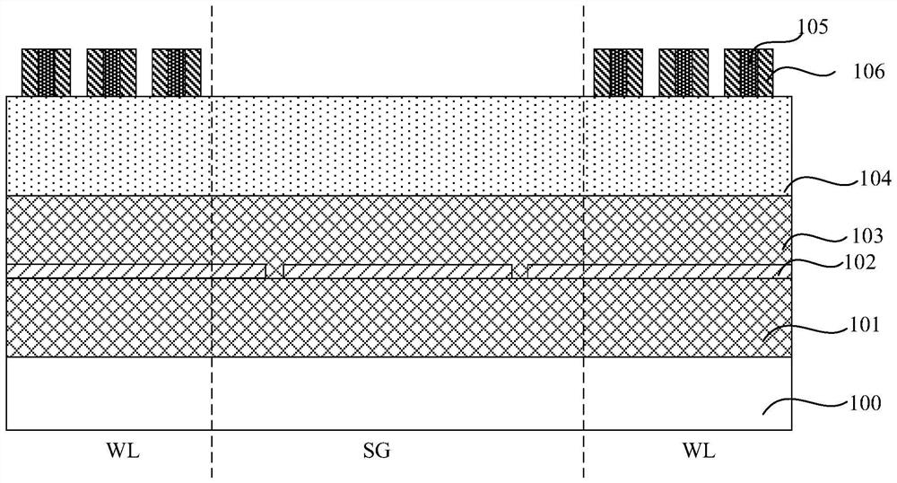
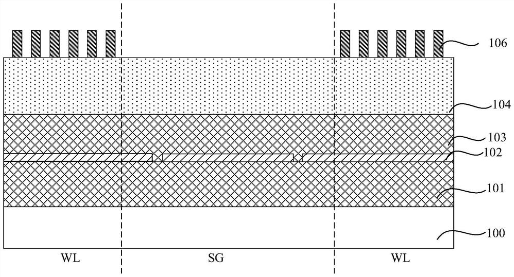
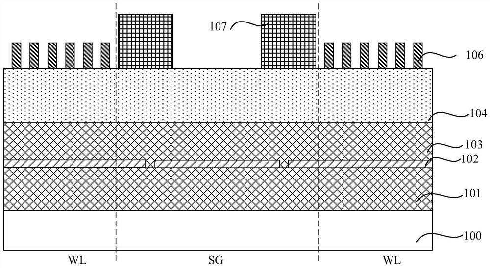
[0045] In the following, a NAND flash memory device is taken as an example to describe in detail the adverse effects of the sparse / dense loading effect of the gate on the performance of the device. Such as Figure 1E As shown, a NAND flash memory device may include: a selection gate (SG, that is, the gate of the selection transistor, the source or drain of the selection transistor is connected to the bit line) 103b and arranged outside the selection gate (SG) 103b A plurality of word lines (WL) 103a, the selection gate (SG) 103b and the word line 103a are formed by connecting the control gates (Control Gate, CG) of the memory cells on the same active area, the selection gate (SG), The word lines (WL) are arranged in parallel, and a corresponding charge storage structure can be provided between each word line 103a and each active area (ACT), so that each intersection of the word line 103a and the active area (ACT) Provide the corresponding storage unit. Usually, the distribut...


PUM


Abstract

The invention provides a semiconductor device and its manufacturing method and mask plate. In the manufacturing method of the semiconductor device, after forming a patterned core layer with a core on the gate dense area and the gate sparse area, the A sidewall is formed on the sidewall of the core, and then the gate layer is etched using the sidewall as a mask to form a first gate on the gate-dense region and a second gate on the gate-sparse region. When the gate base structure is used, the etching load effect between the gate dense area and the gate sparse area can be reduced or even completely avoided, and the uniformity of the critical dimension of the first gate in the formed gate dense area can be improved. The shape of the first gate at the edge is ensured, and then the tops of a plurality of adjacent second gate infrastructure structures on the gate sparse region are connected to form a second gate by means of a connecting gate layer.

Description

technical field [0001] The invention relates to the technical field of integrated circuit manufacturing, in particular to a semiconductor device, a manufacturing method thereof, and a mask plate. Background technique [0002] At present, with the rapid development of ultra-large-scale integrated circuits, the integration of chips is getting higher and higher, and the circuit design size is getting smaller and smaller. The various effects caused by the high density and small size of devices have an increasing impact on the semiconductor manufacturing results. It is outstanding that, especially in the process below the 28nm technology node, the change of the critical dimension (CD, Critical Dimension) of the circuit has more and more influence on the performance of the device. [0003] As we all know, since the gate usually has the smallest physical size in the semiconductor manufacturing process, and the width of the gate is usually the most important critical dimension on th...

Claims


Application Information

Patent Timeline
Patent Type & Authority Patents(China)
IPC IPC(8): H01L27/11524H01L27/11556H01L29/423
CPCH01L29/42328H01L29/42336H10B41/35H10B41/27
Inventor 黄永彬张宏周朝锋周乾
Owner SEMICON MFG INT (SHANGHAI) CORP
Why Eureka
Try Eureka