Preparation method for novel material layer structure of high-frequency circuit board and product thereof

A new type of board and material layer technology, applied in the direction of circuit substrate materials, printed circuit manufacturing, printed circuits, etc., can solve the problem of difficult signal transmission frequency and speed of circuit boards, increased power consumption and signal transmission loss, dielectric constant and Problems such as large loss factor, to achieve the effect of shortening product processing time, improving product performance, and speeding up transmission speed

Inactive Publication Date: 2019-12-13
李龙凯
View PDF0 Cites 0 Cited by
  • Summary
  • Abstract
  • Description
  • Claims
  • Application Information

AI Technical Summary

Problems solved by technology

At present, polyimide (PI) is mainly used as the substrate of flexible boards. However, due to the large dielectric constant and loss factor of PI substrates, large moisture absorption, and poor reliability, the PI flexible boards The high-frequency transmission loss is serious and the structural characteristics are poor, which can no longer adapt to the current high-frequency and high-speed trend
Therefore, with the emergence of new 5G technology products, the signal transmission frequency and speed of existing circuit boards have been difficult to meet the requirements of 5G technology products
[0004] At the same time, in the preparation process, whether it is a traditional multi-layer flexible circuit board or a multi-layer soft-rigid combination board, there are generally many technological processes, complicated production, and problems such as increased power consumption and signal transmission loss in terms of circuit board performance.

Method used


Image

  • Preparation method for novel material layer structure of high-frequency circuit board and product thereof
  • Preparation method for novel material layer structure of high-frequency circuit board and product thereof

Examples


Embodiment 1

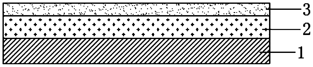
[0027] An embodiment of the present invention provides a method for preparing a new material layer structure of a high-frequency circuit board, including the following steps:

[0028] (1) coating one deck synthetic liquid TFP film on the solidified PI film front;

[0029] (2) Send the cured PI film coated with the synthetic liquid TFP film to the tunnel oven as a whole, and pass through several heating and baking areas in the tunnel oven in sequence at a speed of 0.5-20m / s for segmental baking , forming a semi-cured TFP film on the front side of the cured PI film;

[0030] (3) Copper foil is hot-pressed on the semi-cured TFP film to obtain a new material layer structure on one side of the high-frequency circuit board.

[0031] In the step (2), the several heating and baking zones in the tunnel oven at least include a heating and baking zone, a second heating and baking zone, a third heating and baking zone, and a fourth heating and baking zone , Five-stage heating and baking...

Embodiment 2

[0050] The main difference between this embodiment and Embodiment 1 is:

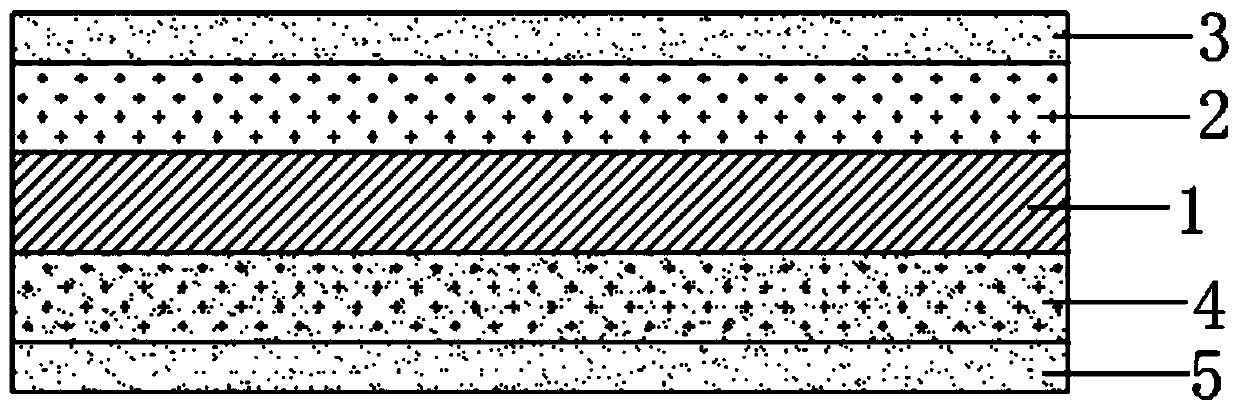
[0051] The step (1) also includes the following steps: coating a layer of synthetic liquid TFP film on the back side of the solidified PI film; after step (2), a semi-cured TFP film is formed on the front and back sides of the solidified PI film; After (3), a double-sided new material layer structure of the high-frequency circuit board is obtained.

[0052] Therefore, the double-sided new material layer structure of the high-frequency circuit board can be prepared by the above method, such as figure 2 As shown, a lower semi-cured TFP film 4 is coated on the back of the cured PI film 1, and a lower copper foil layer 5 is pressed on the lower surface of the lower semi-cured TFP film 4 to form a double-sided new material for high-frequency circuit boards. layer structure. Specifically, after the lower copper foil layer 5 is pressed onto the lower semi-cured TFP film 4 , the lower semi-cured TFP film 4 is...


PUM


Abstract

The invention discloses a preparation method for a novel material layer structure of a high-frequency circuit board. The preparation method comprises the following steps of: (1) coating a cured PI film with a synthetic liquid TFP film, (2) sending the film to a tunnel oven for segmented baking, and forming a semi-cured TFP film on the front surface of the cured PI film, and (3) hot-pressing a copper foil on the semi-cured TFP film to obtain the single-sided novel material layer structure of the high-frequency circuit board. The invention further discloses a novel material layer structure of the high-frequency circuit board, which is prepared by implementing the method. The prepared novel material layer structure of the high-frequency circuit board has the performance of transmitting high-frequency signals at a high speed, can adapt to the high-frequency and high-speed trend from a wireless network to terminal application at present, and is particularly suitable for novel 5G technological products; the material can be used as a manufacturing material of a circuit board to manufacture circuit board structures such as a single-layer circuit board, a multi-layer flexible circuit board,a multi-layer rigid-flex board and the like, thereby bringing great convenience to subsequent manufacturing of the circuit board and simplifying the process.

Description

technical field [0001] The invention relates to the field of circuit boards, in particular to a method for preparing a novel material layer structure of a high-frequency circuit board and a product thereof. Background technique [0002] At present, from the communication network to the terminal application, the communication frequency is comprehensive and high-frequency, and high-speed and large-capacity applications emerge in endlessly. In recent years, with the transition of wireless networks from 4G to 5G, network frequencies have continued to increase. According to the 5G development roadmap shown in relevant materials, the future communication frequency will be upgraded in two stages. The goal of the first stage is to increase the communication frequency to 6GHz before 2020, and the goal of the second stage is to further increase it to 30-60GHz after 2020. In terms of market applications, the signal frequency of terminal antennas such as smartphones continues to incre...

Claims


Application Information

Patent Timeline
Patent Type & Authority Applications(China)
IPC IPC(8): H05K1/03H05K3/00
CPCH05K1/03H05K1/0313H05K1/0353H05K3/0011H05K1/036H05K3/022H05K2201/0195H05K1/095H05K3/007H05K3/025H05K3/384H05K2201/0355
Inventor 李龙凯
Owner 李龙凯
Why Eureka
Try Eureka