Lamination manufacturing process of HDI product

A production process and lamination technology, applied in the direction of multi-layer circuit manufacturing, printed circuit manufacturing, electrical components, etc., can solve the problems of long process production cycle, insufficient filling of holes, complex process, etc., to shorten the delivery time and The effect of quality, improving product yield, and streamlining process flow

Pending Publication Date: 2019-12-13
JIANGSU BOMIN ELECTRONICS
View PDF5 Cites 1 Cited by
  • Summary
  • Abstract
  • Description
  • Claims
  • Application Information

AI Technical Summary

Problems solved by technology

The defects of the existing processing technology are: insufficient fullness of hole filling, too large, partial filling and other difficult-to-observe phenomena; low production capacity, complicated process, long production time; long process production cycle, and easy to produce foreign matter resulting in poor product functionality

Method used


Image

  • Lamination manufacturing process of HDI product

Examples


Embodiment Construction

[0030] The present invention will be further described below in conjunction with specific embodiments.

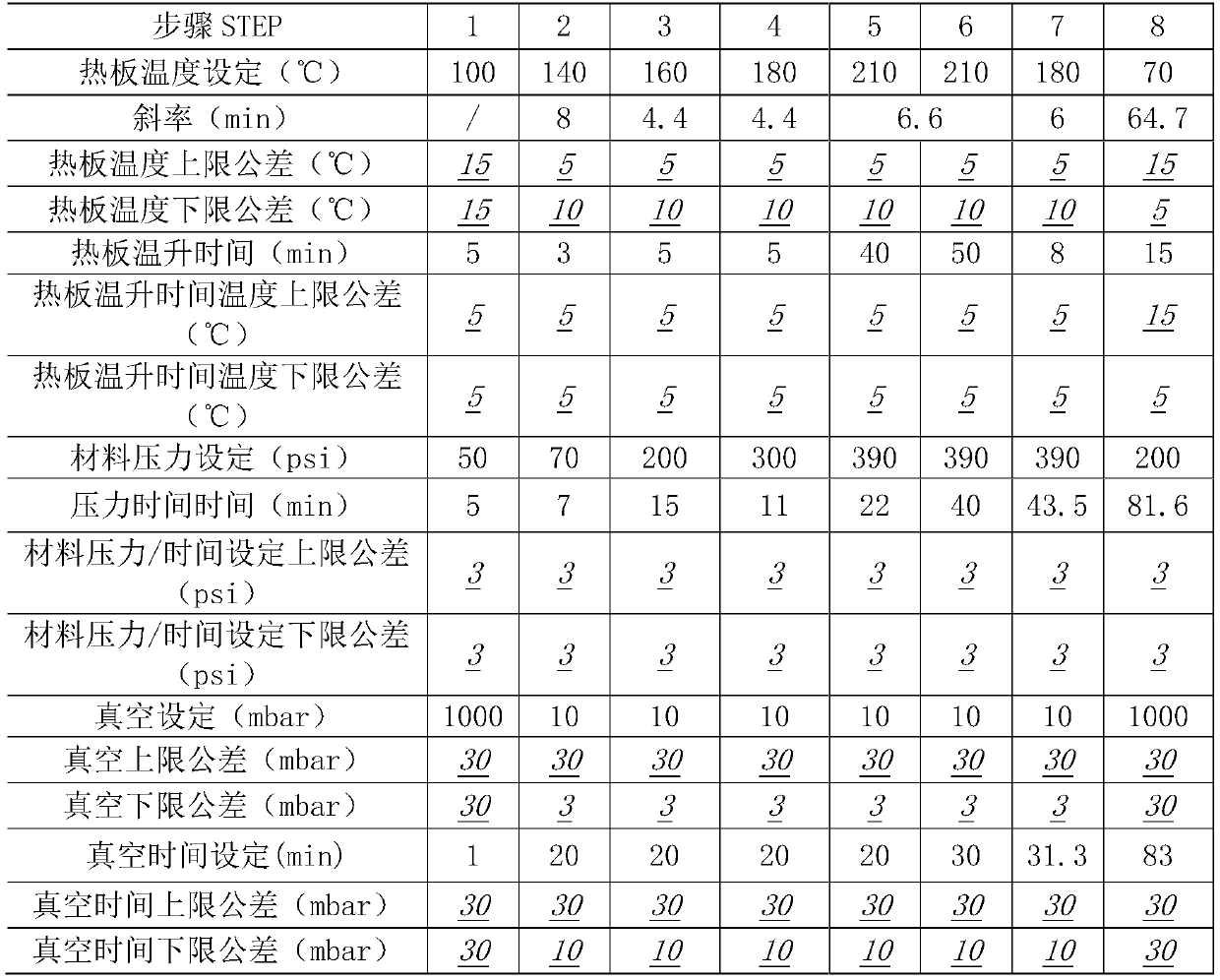
[0031] A lamination process for HDI products includes pre-processing steps, pressing and post-processing steps.

[0032] The pre-processing steps include preparing a core board with through holes. Specifically, the pre-processing steps include cutting, inner layer, inner layer AOI, first pressing, drilling, buried hole electroplating, secondary outer layer wiring, secondary outer layer AOI, and browning. The cutting material is a plate with a substrate thickness of 0.5mm and a base copper thickness of 0.5OZ covering the substrate, and the cutting size is (615±2)mm*(540±2)mm. The inner layer is an inner layer core board made by fabricating inner layer circuit patterns on the copper surface by image transfer. The image transfer method is to align the transmitted line data with the board after the dry film is attached, and then expose. After the image transfer, the unexposed dry ...


PUM


Abstract

The invention provides a lamination manufacturing process of an HDI product, which comprises a preorder processing step, a laminating step and a subsequent processing step, wherein the preorder processing step comprises the preparation of a chip plate with a through hole; the laminating step comprises the sub-steps of laminating the single chip with the through hole through a hot press under a vacuum condition, heating to melt and solidify a prepreg so as to carry out vacuum hole filling on the through hole of the chip; and the subsequent processing step comprises the sub-step of manufacturingthe laminated chip into a finished product. According to the invention, the difficult observation phenomena of insufficient hole filling, oversize hole filling, partial filling and the like are solved; the capacity is improved, the technological process is simplified, and the machining time is shortened; foreign matter sources are reduced, and the product yield is improved; the problems are solved, the equipment, material and labor costs are greatly saved, and the delivery time and quality of the printed circuit board are greatly shortened.

Description

Technical field [0001] The invention belongs to a vacuum filling hole process, and more specifically relates to a lamination manufacturing process of HDI products. Background technique [0002] Existing HDI product vacuum filling hole processing technology includes: plugging process: cutting → inner layer → line inspection → pressing → drilling → electroplating → secondary outer layer line → browning → filling hole (specific material) → finishing Flat → baking → pressing → post-process. The defects of the existing processing technology include: insufficient filling of the hole, too large, filling deviation, etc. which are not easy to observe; low production capacity, complex process, long production time; long process production cycle, and easy to produce foreign matter, which causes poor product functionality . Summary of the invention [0003] The purpose of the present invention is to provide a lamination process for HDI products that can save a lot of equipment, material and...

Claims


Application Information

Patent Timeline
Patent Type & Authority Applications(China)
IPC IPC(8): H05K3/46H05K3/00
CPCH05K3/46H05K3/0094H05K2203/052
Inventor 刘万杰孙守军陈智栋
Owner JIANGSU BOMIN ELECTRONICS
Why Eureka
Try Eureka