Utilizing multilayer gate spacer to reduce erosion of semiconductor fin during spacer patterning

A multi-layer gate and semiconductor technology, applied in semiconductor devices, semiconductor/solid-state device manufacturing, electric solid-state devices, etc.

Pending Publication Date: 2019-12-20
IBM CORP
View PDF8 Cites 0 Cited by
  • Summary
  • Abstract
  • Description
  • Claims
  • Application Information

AI Technical Summary

Problems solved by technology

While the spacer RIE process can be tuned to minimize etch erosion of vertical semiconductor fins formed from silicon (Si) or silicon germanium (SiGe), the selectivity of the RIE p

Method used


Image

  • Utilizing multilayer gate spacer to reduce erosion of semiconductor fin during spacer patterning
  • Utilizing multilayer gate spacer to reduce erosion of semiconductor fin during spacer patterning
  • Utilizing multilayer gate spacer to reduce erosion of semiconductor fin during spacer patterning

Examples


Embodiment Construction

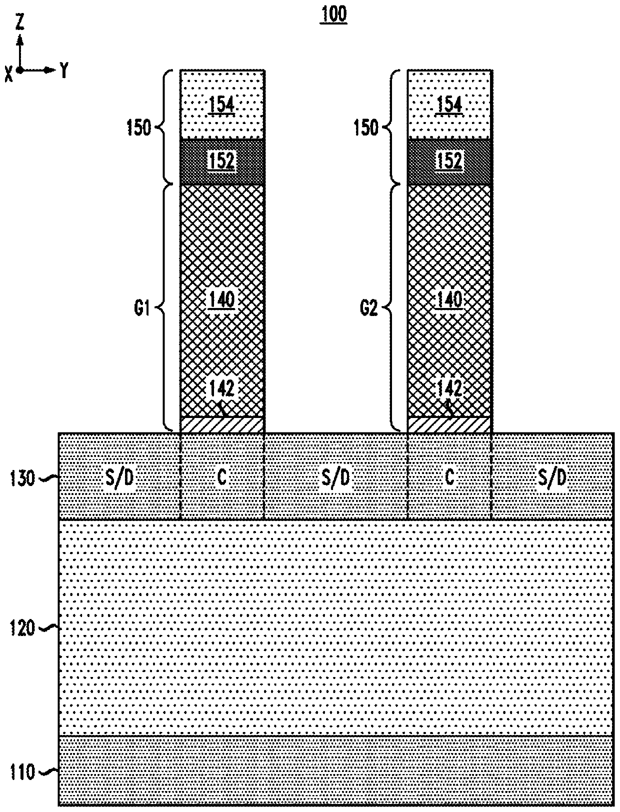
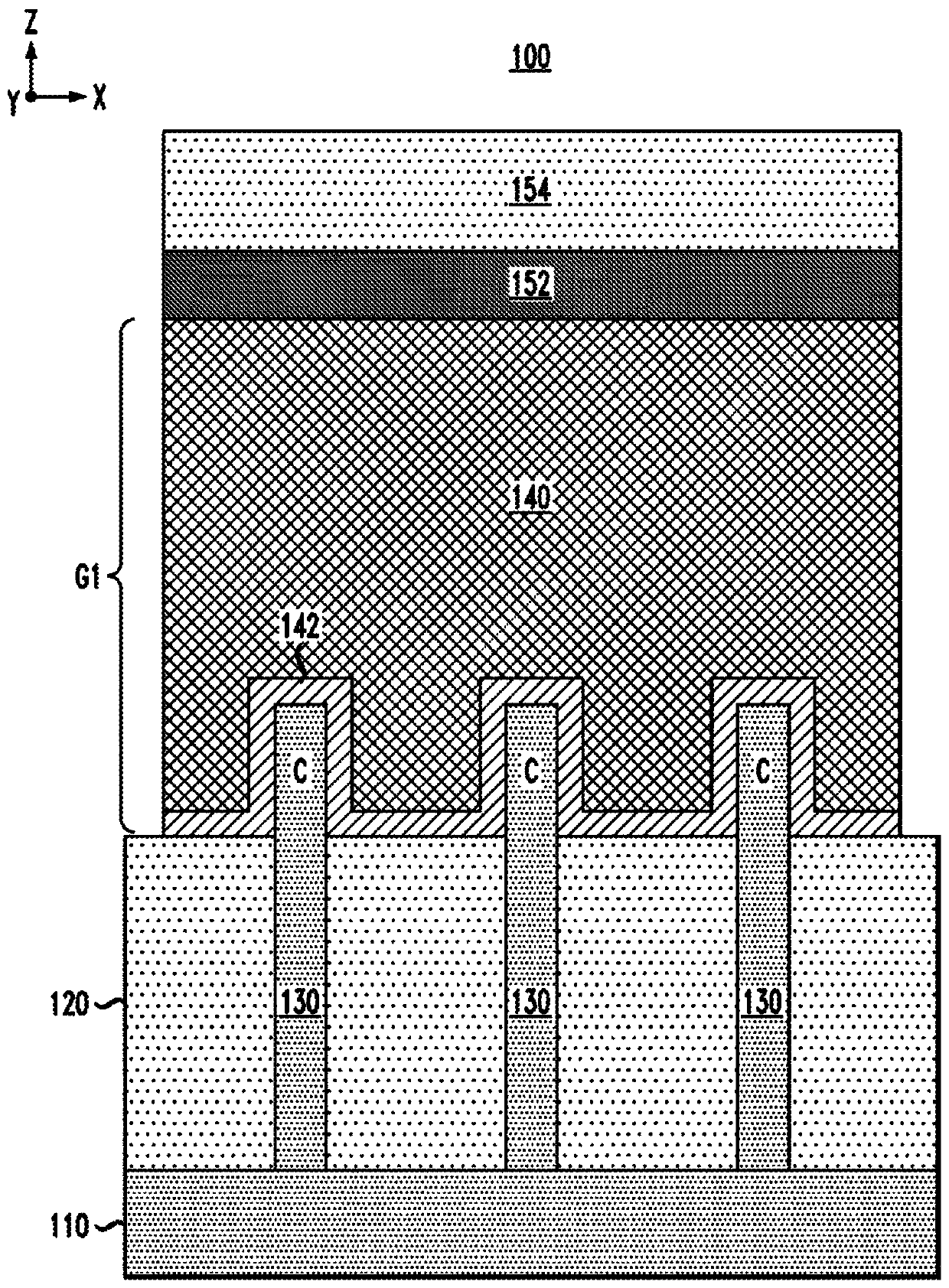
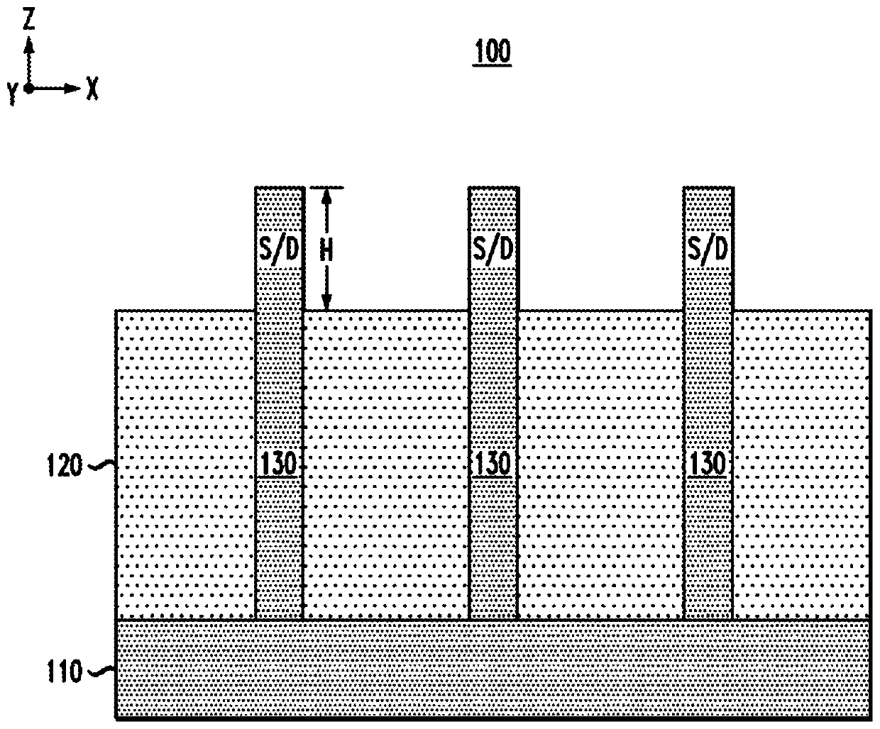
[0015] The embodiments will now be described in further detail with respect to a FinFET device including a multilayer gate isolation and a method for manufacturing a FinFET device, wherein when forming the gate isolation, the multilayer gate isolation is used to prevent or minimize vertical semiconductor fins. corrosion. It should be understood that the various layers, structures and regions shown in the drawings are schematic diagrams that are not drawn to scale. In addition, for ease of explanation, one or more layers, structures, and regions that are commonly used to form semiconductor devices or structures may not be explicitly shown in a given drawing. This does not mean that any layers, structures, and regions that are not explicitly shown are not omitted from the actual semiconductor structure.

[0016] In addition, it should be understood that the embodiments discussed herein are not limited to the specific materials, features, and processing steps shown and described he...


PUM

PropertyMeasurementUnit
Thicknessaaaaaaaaaa
Thicknessaaaaaaaaaa

Abstract

FinFET devices comprising multilayer gate spacers are provided, as well as methods for fabricating FinFET devices in which multilayer gate spacers are utilized to prevent or otherwise minimize the erosion of vertical semiconductor fins when forming the gate spacers. For example, a method for fabricating a semiconductor device comprises forming a dummy gate structure over a portion of a vertical semiconductor fin of a FinFET device, and forming a multilayer gate spacer on the dummy gate structure. The multilayer gate spacer comprises a first dielectric layer and a second dielectric layer, wherein the first dielectric layer has etch selectivity with respect to the vertical semiconductor fin and the second dielectric layer. In one embodiment, the first dielectric layer comprises silicon oxycarbonitride (SiOCN) and the second dielectric layer comprises silicon boron carbon nitride (SiBCN).

Description

Technical field [0001] The present disclosure generally relates to semiconductor manufacturing technology, and in particular, to technology for manufacturing FET (Field Effect Transistor) devices. Background technique [0002] As semiconductor manufacturing technology continues to develop toward smaller design rules and higher integration density (for example, 14nm technology nodes and higher), integrated circuit devices and components become smaller and smaller, which are proposed in layout formation and device optimization Challenge. Currently, FinFET technology is usually used for FET manufacturing, because this type of technology provides an effective CMOS scaling solution for FET manufacturing at 14nm and below technology nodes. The FinFET device includes a three-dimensional fin-shaped FET structure that includes at least one vertical semiconductor fin structure formed on a substrate, a gate structure formed on a portion of the vertical semiconductor fin, and a vertical sem...

Claims


Application Information

Patent Timeline
IPC IPC(8): H01L29/78H01L21/8238
CPCH01L21/823821H01L27/0924H01L29/66545H01L29/66795H01L29/785H01L29/6656
Inventor G·卡夫何虹P·蒙塔尼尼E·米勒S·卡纳卡萨巴帕赛A·格林
Owner IBM CORP
Why Eureka
Try Eureka