A kind of preparation method and application of two-dimensional lead iodide flakes

A lead iodide and flake technology is applied in the field of preparation of lead iodide nanomaterials, and can solve the problems of insufficient size of two-dimensional lead iodide, low yield of two-dimensional nanosheets, rough crystal surface, etc. The effect of high crystal quality and improved device performance

Active Publication Date: 2021-04-27
NANJING UNIV
View PDF4 Cites 0 Cited by
  • Summary
  • Abstract
  • Description
  • Claims
  • Application Information

AI Technical Summary

Problems solved by technology

However, the traditional solution method to prepare two-dimensional lead iodide has problems such as insufficient size (tens of microns), low yield of two-dimensional nanosheets, rough crystal surface, and low crystal quality.

Method used


Image

  • A kind of preparation method and application of two-dimensional lead iodide flakes
  • A kind of preparation method and application of two-dimensional lead iodide flakes
  • A kind of preparation method and application of two-dimensional lead iodide flakes

Examples


Embodiment 1

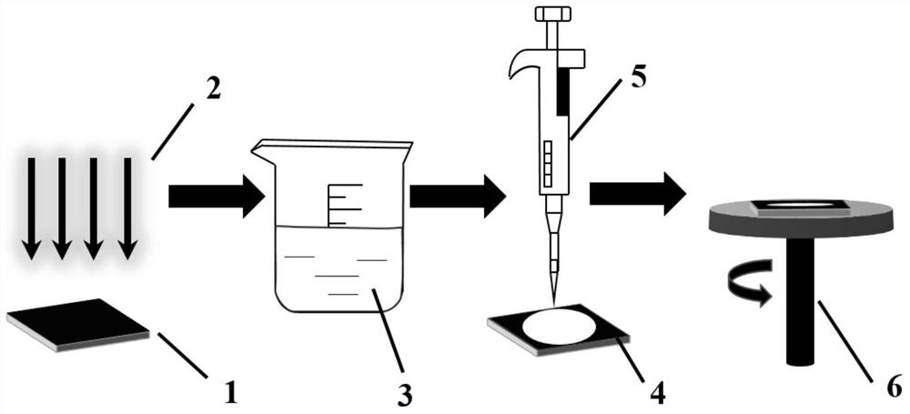
[0034] Cut the silicon wafer with 285nm silicon dioxide into several square pieces of 1cm×1cm, wash and dry it for later use. The cleaned silicon wafer was cleaned for 180 s with a 50W plasma degumming machine, and 100 μL of supersaturated lead iodide aqueous solution (2 mg / mL) was dropped on the treated silicon wafer. The silicon wafer with the lead iodide solution was spin-coated on a spin coater at a speed of 300r / min for 30s, and then the sample was dried at 25°C to obtain a two-dimensional lead iodide flake.

Embodiment 2

[0036] Cut the silicon wafer with 285nm silicon dioxide into several square pieces of 1cm×1cm, wash and dry it for later use. The cleaned silicon wafer was cleaned for 120 s with a 180W plasma degumming machine, and 50 μL of supersaturated lead iodide aqueous solution (2 mg / mL) was dropped onto the treated silicon wafer. The silicon wafer with the lead iodide solution was spin-coated on a spin coater at a speed of 300r / min for 30s, and then the sample was dried at 25°C to obtain a two-dimensional lead iodide flake.

Embodiment 3

[0038] Cut the silicon wafer with 285nm silicon dioxide into several square pieces of 1cm×1cm, wash and dry it for later use. The cleaned silicon wafer was cleaned with a 400W plasma degumming machine for 60 s, and 300 μL of supersaturated lead iodide aqueous solution (4 mg / mL) was dropped on the treated silicon wafer. The silicon wafer with the lead iodide solution was spin-coated on a spin coater at a speed of 1000r / min for 20s, and then the sample was dried at 50°C to obtain a two-dimensional lead iodide flake.


PUM


Abstract

The invention discloses a preparation method and application of a two-dimensional lead iodide flake. The preparation method comprises the following steps: cleaning the substrate; adding a quantitative supersaturated lead iodide aqueous solution dropwise on the cleaned substrate; Two-dimensional lead iodide flakes are obtained after volatilization. The preparation method of the present invention is simple in operation, low in cost, and environmentally friendly, and can quickly and high-yield prepare two-dimensional lead iodide flakes, and the prepared two-dimensional lead iodide flakes have large size, smooth surface, and high crystal quality, and can be processed applied to photodetectors.

Description

technical field [0001] The invention relates to the technical field of two-dimensional nanomaterials, in particular to a preparation method and application of a lead iodide nanomaterial. Background technique [0002] Two-dimensional materials refer to layered nanomaterials that are nanometer-sized (less than 100 nm) in only one dimension. Atoms are chemically bonded in a two-dimensional plane, and electrons move freely in the plane. When materials are thinned to two-dimensional dimensions, they often exhibit numerous unique and excellent properties that are not specific to bulk materials. The unique mechanical, electrical, optical, thermal, and magnetic properties of these two-dimensional materials have attracted extensive attention from academia and industry. [0003] Lead iodide is a layered material, the layers are connected by van der Waals force, and the layers are connected by iodine and lead ionic bonds. The bandgap of lead iodide is 2.2-2.55eV, and the bandgap will...

Claims


Application Information

Patent Timeline
Patent Type & Authority Patents(China)
IPC IPC(8): H01L31/18
CPCH01L31/18Y02P70/50
Inventor 吴明泽万祖腾夏奕东宁兴海
Owner NANJING UNIV
Why Eureka
Try Eureka