
Photoetching process method

A lithography process and process technology, applied in the field of lithography process, can solve the problems of image defocus, affecting exposure resolution and process window, and high photoresist height, so as to prevent defocus, improve resolution and process window , Increase the effect of depth of focus

Inactive Publication Date: 2019-12-31
SHANGHAI HUALI INTEGRATED CIRCUTE MFG CO LTD
View PDF6 Cites 3 Cited by
  • Summary
  • Abstract
  • Description
  • Claims
  • Application Information

AI Technical Summary

Problems solved by technology

With the decrease of the line width and the increase of the thickness of the photoresist required by the process, the height of the photoresist is often greater than the depth of focus, so that the bottom or top of the photoresist is not within the range of the depth of focus, resulting in loss of graphics. focus, which affects the resolution and process window of the exposure
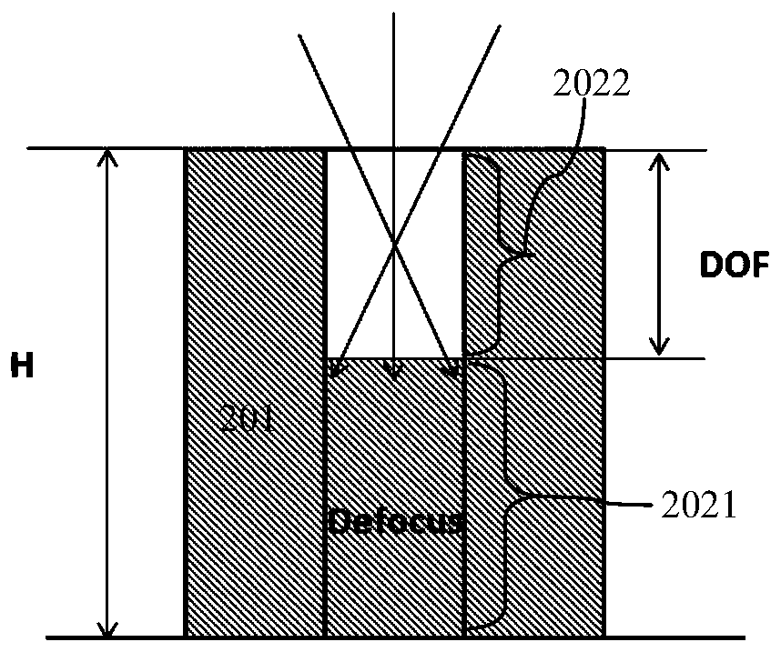
like figure 2 As shown, it is a schematic diagram of the photoresist defocus (defocus) when the photoresist height is greater than the depth of focus in the existing photolithography process; The sub-layer 2022 of 201 from the surface to the thickness within the range of DOF is exposed, and the sub-layer 2021 at the bottom of the sub-layer 2022 is an out-of-focus part. The sub-layer 2021 is also represented by Defocus, and the sub-layer 2021 cannot achieve good exposure, which will cause Graphics do not meet requirements

Method used


Image

  • Photoetching process method
  • Photoetching process method
  • Photoetching process method

Examples


no. 1 example

[0042] The photolithography process method of the first embodiment of the present invention:

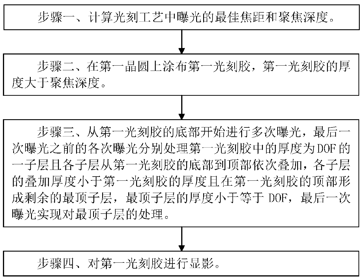
[0043] Such as image 3 Shown is the flowchart of the photolithography process method of the first embodiment of the present invention; as Figure 4A to Figure 4B As shown, it is a schematic diagram of the photoresist structure in the exposure process of the photolithography process method of the first embodiment of the present invention; the photolithography process method of the first embodiment of the present invention includes steps:

[0044] Step 1. Calculating the optimal focal length and depth of focus of exposure in the photolithography process; let the optimal focal length be f and the depth of focus be DOF.

[0045] Step 1 is implemented in the following sub-steps:

[0046] Step 11, coating a second photoresist on the second wafer, the thickness of the second photoresist is H1, and H1 is smaller than H.

[0047] The second wafer can be the subsequent first wafer or other...

no. 2 example

[0066] The photolithography process method of the second embodiment of the present invention:

[0067] Such as Figure 5A to Figure 5C As shown, it is a schematic diagram of the photoresist structure during the exposure process of the photolithography process method of the second embodiment of the present invention; the difference between the photolithography process method of the second embodiment of the present invention and the photolithography process method of the first embodiment of the present invention Therefore, the photolithography process method in the second embodiment of the present invention has the following features:

[0068] H=nDOF and n>2, n exposures are carried out in step 3; the focal length of the kth exposure is fk, and k is any integer between 1 and n; then:

[0069] fk=f+H / 2-k*DOF.

[0070] Figure 5A Corresponding to the first exposure, the first exposure implements exposure to the sub-layer 21 in the photoresist 1 , and the thickness of the sub-la...

no. 3 example

[0077] The photolithography process method of the third embodiment of the present invention:

[0078] The difference between the lithography process method of the third embodiment of the present invention and the lithography process method of the first embodiment of the present invention is that the lithography process method of the third embodiment of the present invention has the following features:

[0079] H in step 2 is changed so that H is less than or equal to DOF; at this time, an exposure is performed in step 3, and f measured in step 1 is used for the exposure. Compared with the prior art, the advantage of the third embodiment of the present invention is that the photoresist 1 can be exposed at the best focal length, thereby increasing the process window.


PUM


Abstract

The invention discloses a photoetching process method. The photoetching process method comprises the following steps: 1, an optimal focal length and a focusing depth of exposure in a photoetching process are calculated; 2, a first photoresist is applied to a first wafer, wherein the thickness of the first photoresist is greater than the focusing depth; 3, exposure for multiple times is carried outfrom the bottom of the first photoresist, wherein each time of exposure before the last-time exposure is to process a sub-layer with the thickness of DOF in the first photoresist, the sub-layers aresuperposed sequentially from the bottom to the top of the first photoresist, the superposition thickness of the sub-layers is smaller than the thickness of the first photoresist, the remaining topmostsub-layer is formed at the top of the first photoresist, the thickness of the topmost sub-layer is smaller than or equal to the DOF, and the topmost sub-layer is processed through the last-time exposure; and 4, the first photoresist is developed. The focusing depth of the thick photoresist process can be increased, and the resolution and the process window are improved.

Description

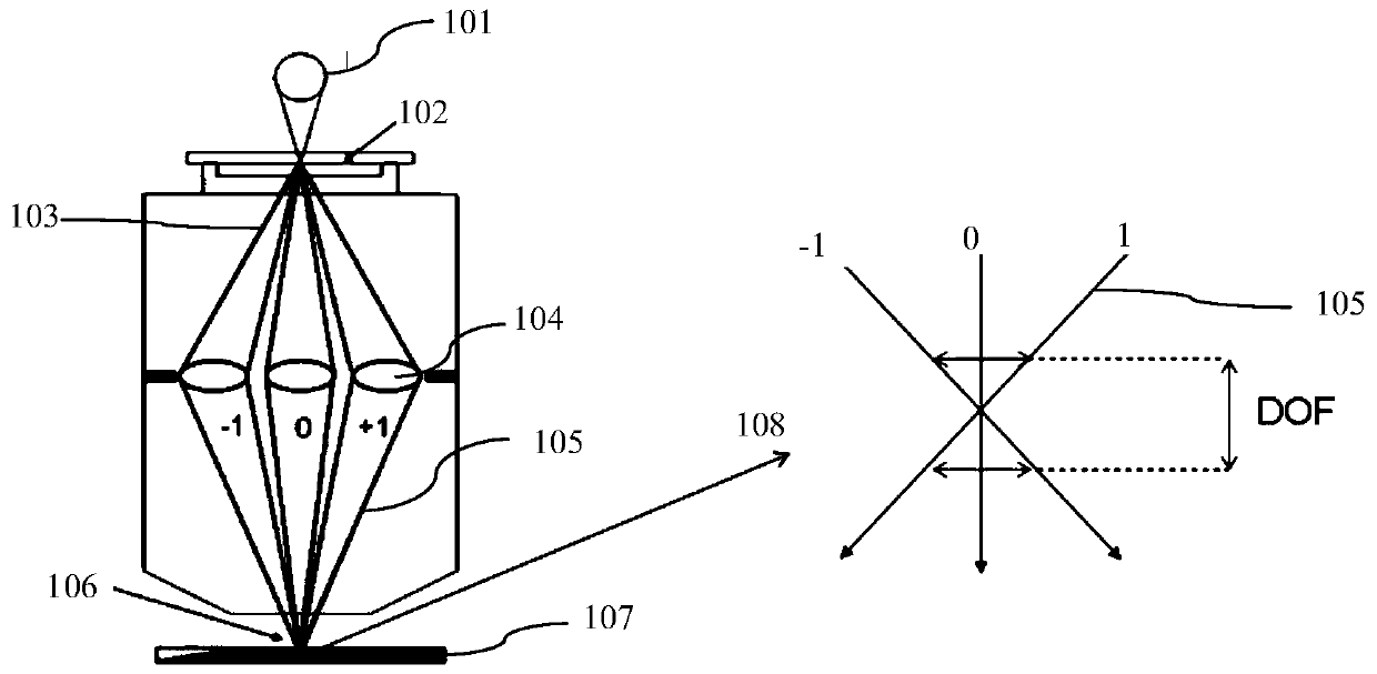
technical field [0001] The invention relates to a semiconductor integrated circuit manufacturing method, in particular to a photolithography process method. Background technique [0002] Photolithography is the process of transferring the pattern prepared in advance on the mask (Mask) to the substrate by using the principle of photochemical reaction. Depth-of-focus (DOF) is an important parameter to measure the lithography process window, which marks the relationship between the imaging quality of the exposure system and the position of the wafer surface. Within the range of depth of focus, the quality of exposure imaging can be guaranteed. [0003] Such as figure 1 As shown, it is a schematic diagram of the depth of focus exposed in the photolithography process; in the exposure process, after the light source 101 passes through the mask (Mask) 102, the pattern on the mask 102 will diffract the light and form a corresponding diffraction image (Diffracted Image) 103, after...

Claims


Application Information

Patent Timeline
Patent Type & Authority Applications(China)
IPC IPC(8): G03F7/20G03F9/00
CPCG03F7/70466G03F7/70641G03F9/7026
Inventor 官锡俊
Owner SHANGHAI HUALI INTEGRATED CIRCUTE MFG CO LTD
Learn More