A kind of preparation method of Ge-based CMOS transistor

A technology of transistors and metal layers, applied in the direction of transistors, semiconductor/solid-state device manufacturing, semiconductor devices, etc., can solve problems affecting device performance, excessive source-drain contact resistance, low N-type impurity activation concentration, etc.

Active Publication Date: 2021-09-14
INST OF MICROELECTRONICS CHINESE ACAD OF SCI
View PDF2 Cites 0 Cited by
  • Summary
  • Abstract
  • Description
  • Claims
  • Application Information

AI Technical Summary

Problems solved by technology

[0004] In order to overcome the low N-type impurity activation concentration existing in existing Ge-based devices, and the Fermi level pinning effect caused by the contact between metal and Ge, resulting in excessive source-drain contact resistance, thereby affecting the technical problems of device performance, the present invention provides A kind of Ge base CMOS (complementary metal oxide semiconductor) transistor preparation method

Method used


Image

  • A kind of preparation method of Ge-based CMOS transistor
  • A kind of preparation method of Ge-based CMOS transistor
  • A kind of preparation method of Ge-based CMOS transistor

Examples


Embodiment Construction

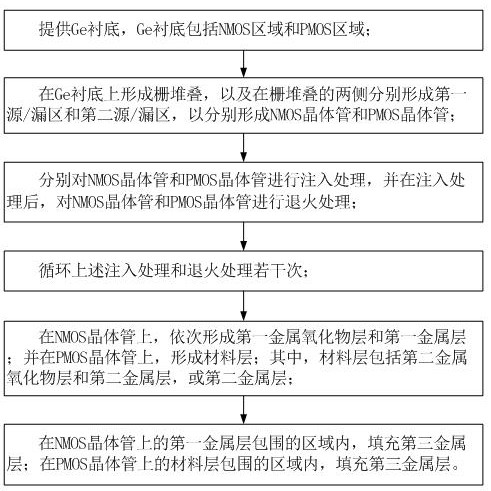
[0043] The specific implementation manners according to the present invention will be described below in conjunction with the accompanying drawings.

[0044] In the following description, many specific details are set forth in order to fully understand the present invention, but the present invention can also be implemented in other ways different from those described here, therefore, the present invention is not limited to the specific embodiments disclosed below limit.

[0045] Ge material has high and symmetrical carrier mobility, which can provide larger driving current and faster switching speed; at the same time, the forbidden band width of Ge is smaller than that of Si, and the required driving voltage is lower. Advantages, making it one of the most promising development directions for high-performance MOS devices.

[0046] However, there are still many problems to be solved in Ge-based devices, such as: low N-type impurity activation concentration, that is, in the Ge ...


PUM

PropertyMeasurementUnit
thicknessaaaaaaaaaa
thicknessaaaaaaaaaa

Abstract

The invention discloses a method for preparing a Ge-based CMOS transistor, which comprises the steps of: providing a Ge substrate; forming a gate stack on the Ge substrate, and forming a first source / drain region and a second source / drain region on both sides of the gate stack Drain regions to form NMOS and PMOS transistors respectively; Implantation treatment is performed on the NMOS and PMOS transistors respectively, and after the implantation treatment, annealing treatment is performed on the NMOS and PMOS transistors; the above-mentioned injection treatment and annealing treatment are cycled several times; on the NMOS transistor , forming a first metal oxide layer and a first metal layer in sequence; and forming a material layer on the PMOS transistor; wherein, the material layer includes a second metal oxide layer and a second metal layer, or a second metal layer; on the NMOS transistor The area surrounded by the first metal layer on the transistor is filled with the third metal layer; the area surrounded by the material layer on the PMOS transistor is filled with the third metal layer. The Ge-based CMOS transistor preparation method provided by the invention reduces the source-drain contact resistance of the CMOS transistor and improves the performance of the CMOS transistor.

Description

technical field [0001] The invention relates to the technical field of semiconductors, in particular to a method for preparing a Ge-based CMOS transistor. Background technique [0002] Ge (germanium) material has high and symmetrical carrier mobility, which can provide larger driving current and faster switching speed; at the same time, the forbidden band width of Ge is smaller than that of Si (silicon), and the required driving voltage is higher. Low, the advantages of Ge material itself make it one of the most promising development directions for high-performance MOS devices. [0003] However, there are still many problems to be solved in Ge-based devices, such as: low N-type impurity activation concentration, that is, in the Ge substrate, the electron concentration activated by N-type impurities is difficult to increase; and there is a Fermi energy in the contact between the metal and Ge. The level pinning effect will lead to excessive source-drain contact resistance, th...

Claims


Application Information

Patent Timeline
Patent Type & Authority Patents(China)
IPC IPC(8): H01L27/092H01L21/8238H01L29/16
CPCH01L21/823814H01L27/092H01L29/16
Inventor 毛淑娟罗军许静
Owner INST OF MICROELECTRONICS CHINESE ACAD OF SCI
Why Eureka
Try Eureka