

High-precision ADC input signal control circuit
An input signal and control circuit technology, applied in electrical components, physical parameter compensation/prevention, analog-to-digital converters, etc., can solve the problems of control voltage attenuation, large chip area, difficult circuit stabilization, etc. The effect of low chip area and waveform distortion
- Summary
- Abstract
- Description
- Claims
- Application Information
AI Technical Summary
Problems solved by technology
Method used
Image

Examples
Embodiment Construction
[0026] The following will clearly and completely describe the technical solutions in the embodiments of the present invention with reference to the accompanying drawings in the embodiments of the present invention. Obviously, the described embodiments are only some, not all, embodiments of the present invention. Based on the embodiments of the present invention, all other embodiments obtained by persons of ordinary skill in the art without creative efforts fall within the protection scope of the present invention.
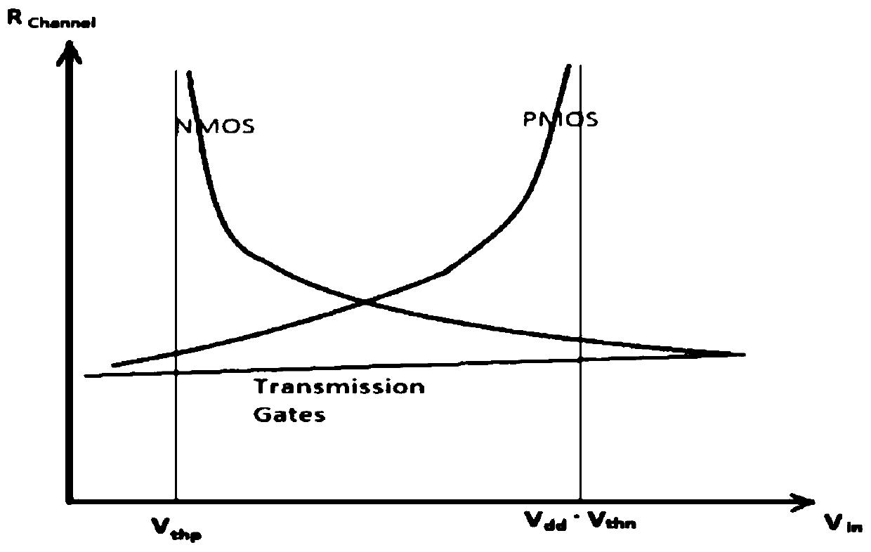
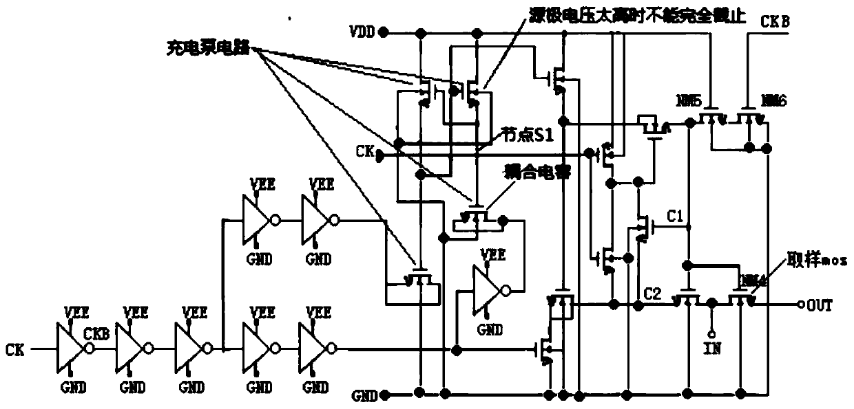
[0027] see Figure 1-8 , the present invention provides a technical solution: a high-precision ADC input signal control circuit, including a clock control switch and forward and reverse biased diodes, and a charging and discharging circuit formed by the clock control switch and forward and reverse biased diodes controls the voltage of the clock Level, so that the switch control signal changes synchronously with the input signal voltage level, reducing the distortio...
PUM
 Abstract
Description
Claims
Application Information