Stacked packaging process for semiconductor device and semiconductor device

A packaging process and semiconductor technology, applied in the direction of electrical components, impedance networks, etc., can solve problems such as large product thickness, difficult process, and complicated wiring

Active Publication Date: 2020-01-03
HUZHOU JIANWENLU TECH INC
View PDF4 Cites 6 Cited by
  • Summary
  • Abstract
  • Description
  • Claims
  • Application Information

AI Technical Summary

Problems solved by technology

When integrated into the module by wafer bonding packaging, it is not sensitive to injection pressure, the product thickness is large, and the wiring is complicated and requires TSV conduction, so the process control is difficult and the cost is high.
The thin film packaging method can make the product very thin, but it involves multiple photolithography and thin film deposition processes, which makes the process difficult and costly, and is sensitive to injection molding pressure, so it cannot be used for the stacked packaging of two dies.

Method used


Image

  • Stacked packaging process for semiconductor device and semiconductor device
  • Stacked packaging process for semiconductor device and semiconductor device
  • Stacked packaging process for semiconductor device and semiconductor device

Examples


Embodiment Construction

[0039]The application will be further described in detail below in conjunction with the accompanying drawings and embodiments. It should be understood that the specific embodiments described here are only used to explain related inventions, rather than to limit the invention. It should also be noted that, for the convenience of description, only the parts related to the related invention are shown in the drawings.

[0040] It should be noted that, in the case of no conflict, the embodiments in the present application and the features in the embodiments can be combined with each other. The present application will be described in detail below with reference to the accompanying drawings and embodiments.

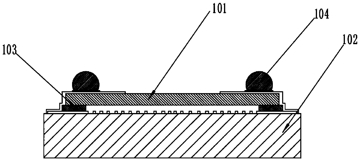
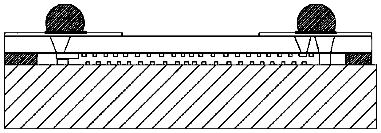
[0041] Figure 1a and Figure 1b A schematic diagram showing a WLP wafer-level package filter in the prior art using a wafer-bonded package structure. There are two main structures and processing methods for the filter to be packaged by wafer bonding, such as Figure 1a In t...


PUM

PropertyMeasurementUnit
Widthaaaaaaaaaa
Opening widthaaaaaaaaaa
Thicknessaaaaaaaaaa

Abstract

The embodiment of the invention provides a superposition packaging process for a semiconductor device and the semiconductor device, and the process comprises the following steps: preparing a main wafer, and reserving a packaging bonding region on the front surface of the main wafer; preparing an auxiliary wafer, reserving a packaging bonding area on the front surface of the auxiliary wafer, and processing a plurality of grooves on the front surface of the auxiliary wafer; bonding the packaging bonding areas of the main wafer and the auxiliary wafer together to realize superposition of the twowafers; and grinding or thinning the back surface of the auxiliary wafer until at least part of the area of the main wafer is exposed out of the groove. The process is very suitable for manufacturingtwo-in-one and duplexer chips, and is particularly suitable for manufacturing acoustic wave filters. The invention provides a novel wafer-level stacking packaging structure, wafer-level packaging in adie stacking mode is achieved, the structure has the functions of two chips, the packaging size and the chip area can be greatly reduced, and the size of the structure is only about 60% compared withthe sizes of the two independently packaged chips.

Description

technical field [0001] The present application belongs to the field of semiconductor devices, in particular to an overlay packaging process for semiconductor devices and semiconductor devices. Background technique [0002] As a semiconductor device, filters are widely used in many wireless cellular terminals (including 2G / 3G / 4G / 5G mobile phones, WiFi, Pad, smart watches, IOT, automobiles and other terminal scenarios). The transmitting end (TX) and receiving end (RS) of the mobile communication system must be filtered by the filter before they can play a role. Since the operating frequency band is generally 800MHz-2GHz and the bandwidth is 17MHz-30MHz, the filter is required to have low insertion loss. , High stop band suppression and high image attenuation, high power withstand, low cost, miniaturization and so on. Compared with piezoelectric ceramic filters and monolithic crystal filters, surface acoustic wave filters have obvious advantages in terms of operating frequency...

Claims


Application Information

Patent Timeline
IPC IPC(8): H03H3/10H03H3/007
CPCH03H3/007H03H3/10
Inventor 李林萍盛荆浩江舟
Owner HUZHOU JIANWENLU TECH INC
Why Eureka
Try Eureka