Supercharge Your Innovation With Domain-Expert AI Agents!

Manufacture method of liquid crystal on silicon device and liquid crystal on silicon device, and wavelength selective switch

A silicon-based liquid crystal and a manufacturing method technology are applied in the field of silicon-based liquid crystal devices, the manufacture of silicon-based liquid crystal devices, and wavelength selective switches, and can solve the problems of poor surface flatness of passivation layer, poor surface flatness of alignment film, uneven liquid crystal characteristics, etc. problems, to achieve the effect of improving surface flatness, high surface flatness, and improving product quality

Pending Publication Date: 2020-01-07
SHENZHEN KECHUANG DIGITAL DISPLAY TECH
View PDF11 Cites 0 Cited by
  • Summary
  • Abstract
  • Description
  • Claims
  • Application Information

AI Technical Summary

Problems solved by technology

In order to protect the bottom electrodes, it is usually necessary to form a passivation layer covering a plurality of bottom electrodes and the intervals between adjacent bottom electrodes on the silicon wafer. The alignment film is formed on the passivation layer. However, since the bottom electrodes are arranged at intervals , the passivation layer will form a depression corresponding to the interval between adjacent bottom electrodes, making the surface flatness of the passivation layer poor, which in turn leads to poor surface flatness of the alignment film, and cannot make the liquid crystal molecules in the liquid crystal layer have continuity The arrangement direction of the liquid crystal leads to non-uniform characteristics of the liquid crystal, which cannot meet the characteristic requirements applied to the wavelength selective switch

Method used


Image

  • Manufacture method of liquid crystal on silicon device and liquid crystal on silicon device, and wavelength selective switch
  • Manufacture method of liquid crystal on silicon device and liquid crystal on silicon device, and wavelength selective switch
  • Manufacture method of liquid crystal on silicon device and liquid crystal on silicon device, and wavelength selective switch

Examples


Embodiment Construction

[0043] In order to further illustrate the technical means adopted by the present invention and its effects, the following describes in detail in conjunction with preferred embodiments of the present invention and accompanying drawings.

[0044] see Figure 1 to Figure 9 , the invention provides a method for manufacturing a silicon-based liquid crystal device, comprising the steps of:

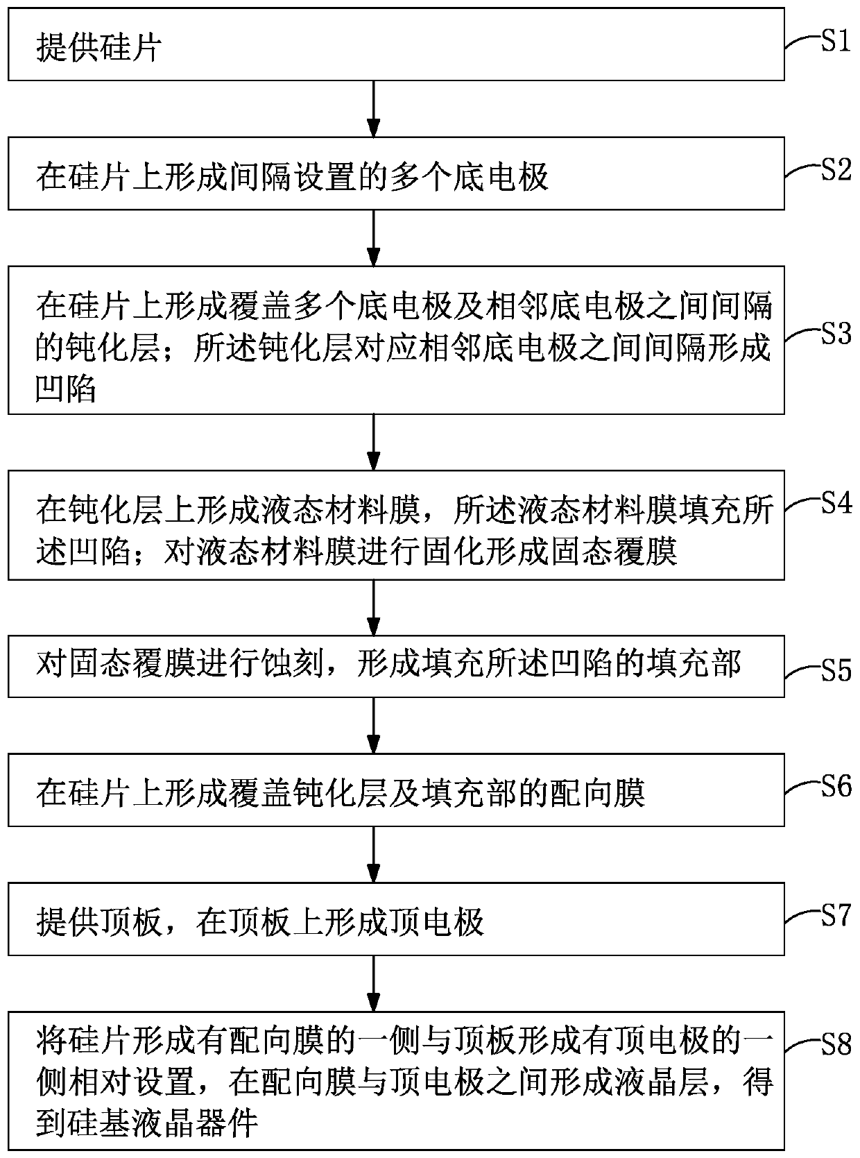
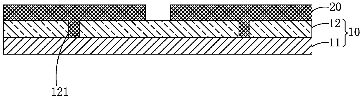
[0045] Step S1, please refer to figure 2 , providing a silicon wafer 10 .

[0046] Specifically, the silicon chip 10 includes a bottom circuit 11 and an insulating layer 12 disposed on the bottom circuit 11 , and the insulating layer 12 is provided with a plurality of via holes 121 arranged at intervals.

[0047] Step S2, please refer to figure 2 , forming a plurality of bottom electrodes 20 arranged at intervals on the silicon wafer 10 .

[0048] Specifically, a plurality of bottom electrodes 20 are formed on the insulating layer 12 , and each bottom electrode 20 is correspondingly connec...


PUM

PropertyMeasurementUnit
thicknessaaaaaaaaaa
thicknessaaaaaaaaaa
thicknessaaaaaaaaaa

Abstract

The invention provides a manufacture method of a liquid crystal on silicon device and the liquid crystal on silicon device, and a wavelength selective switch. The manufacture method of the liquid crystal on silicon device comprises steps of forming a liquid material film on a passivation layer covering a space between a bottom electrode and an adjacent bottom electrode, filling a dent on the passivation layer by using the liquid material film, then solidifying the liquid material film so as to form a solid covering film, etching the solid covering film so as to form a filling part filling thedent, then forming an alignment film covering the passivation layer and the filling part on a silicon wafer. The filling part fills the dent in the surface of the passivation layer, so that the alignment film prepared in later stage has a flatter surface, liquid crystal molecules in the liquid crystal layer are arranged in a continuous direction, the liquid crystal is homogeneous in property, andproducts like the wavelength selective switch have higher quality.

Description

technical field [0001] The invention relates to the technical field of optical equipment, in particular to a method for manufacturing a silicon-based liquid crystal device, a silicon-based liquid crystal device, and a wavelength selection switch. Background technique [0002] The wavelength selective switch (Wavelength Selective Switch, WSS) is the core optoelectronic device of the reconfigurable optical add-drop multiplexer (Reconfigurable Optical Add-Drop Multiplexer, ROADM), which can realize the optical signal switching of any wavelength or any combination of wavelengths on any port , attenuation or blocking, is one of the key products in the current optical communication industry. [0003] The wavelength selective switch generally includes an optical fiber array, a shaping lens, a diffraction grating, a converging lens, and a control chip. The optical signal input by the light array is collimated by the shaping lens, the light spot is shaped, and then passes through the...

Claims


Application Information

Patent Timeline
Patent Type & Authority Applications(China)
IPC IPC(8): G02F1/13G02F1/1337G02F1/1362
CPCG02F1/1303G02F1/1337G02F1/133711G02F1/136277
Inventor 李方红常嘉兴
Owner SHENZHEN KECHUANG DIGITAL DISPLAY TECH
Features
  • R&D
  • Intellectual Property
  • Life Sciences
  • Materials
  • Tech Scout
  • Unparalleled Data Quality
  • Higher Quality Content
  • 60% Fewer Hallucinations
Learn More