
Trench MOSFET and manufacturing method thereof

A manufacturing method and groove technology, applied in semiconductor/solid-state device manufacturing, electrical components, circuits, etc., can solve the problems of not lowering the withstand voltage, reducing the specific on-resistance of SGTMOS, and increasing the specific on-resistance, achieving a reduction in the ratio Effects of on-resistance, increased doping concentration, and improved withstand voltage

Pending Publication Date: 2020-01-10
WUXI CHINA RESOURCES HUAJING MICROELECTRONICS
View PDF3 Cites 2 Cited by
  • Summary
  • Abstract
  • Description
  • Claims
  • Application Information

AI Technical Summary

Problems solved by technology

The doping concentration of the epitaxial layer of the SGTMOS in the prior art is constant, and the withstand voltage of the SGTMOS can be improved by reducing the doping concentration of the epitaxial layer, but it will also cause the specific on-resistance of the SGTMOS (conduction per unit area on-resistance) increases
Therefore, the existing SGTMOS cannot further increase the withstand voltage of the SGTMOS without increasing the specific on-resistance, nor can it reduce the specific on-resistance of the SGTMOS without reducing the withstand voltage.

Method used


Image

  • Trench MOSFET and manufacturing method thereof
  • Trench MOSFET and manufacturing method thereof
  • Trench MOSFET and manufacturing method thereof

Examples


Embodiment Construction

[0057] Reference will now be made in detail to the exemplary embodiments, examples of which are illustrated in the accompanying drawings. When the following description refers to the accompanying drawings, the same numerals in different drawings refer to the same or similar elements unless otherwise indicated. The implementations described in the following exemplary embodiments do not represent all implementations consistent with this application. Rather, they are merely examples of means consistent with aspects of the present application as recited in the appended claims.

[0058] The terminology used in this application is for the purpose of describing particular embodiments only, and is not intended to limit the application. Unless otherwise defined, the technical terms or scientific terms used in the present application shall have the common meanings understood by those skilled in the art to which the present invention belongs. Words such as "one" or "one" used in the sp...


PUM

PropertyMeasurementUnit
thicknessaaaaaaaaaa

Abstract

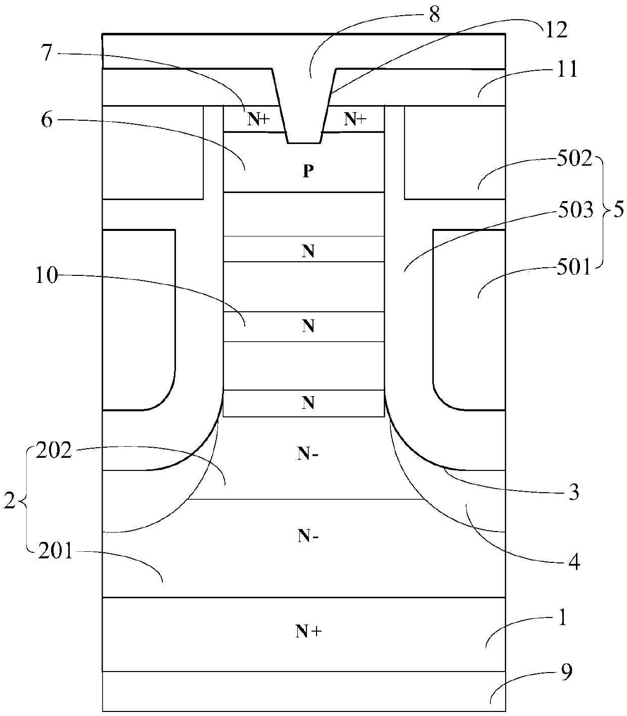
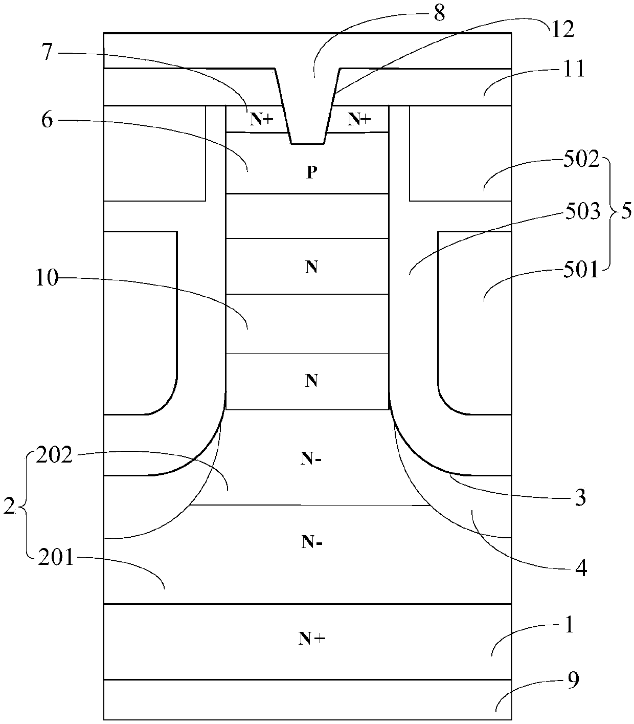
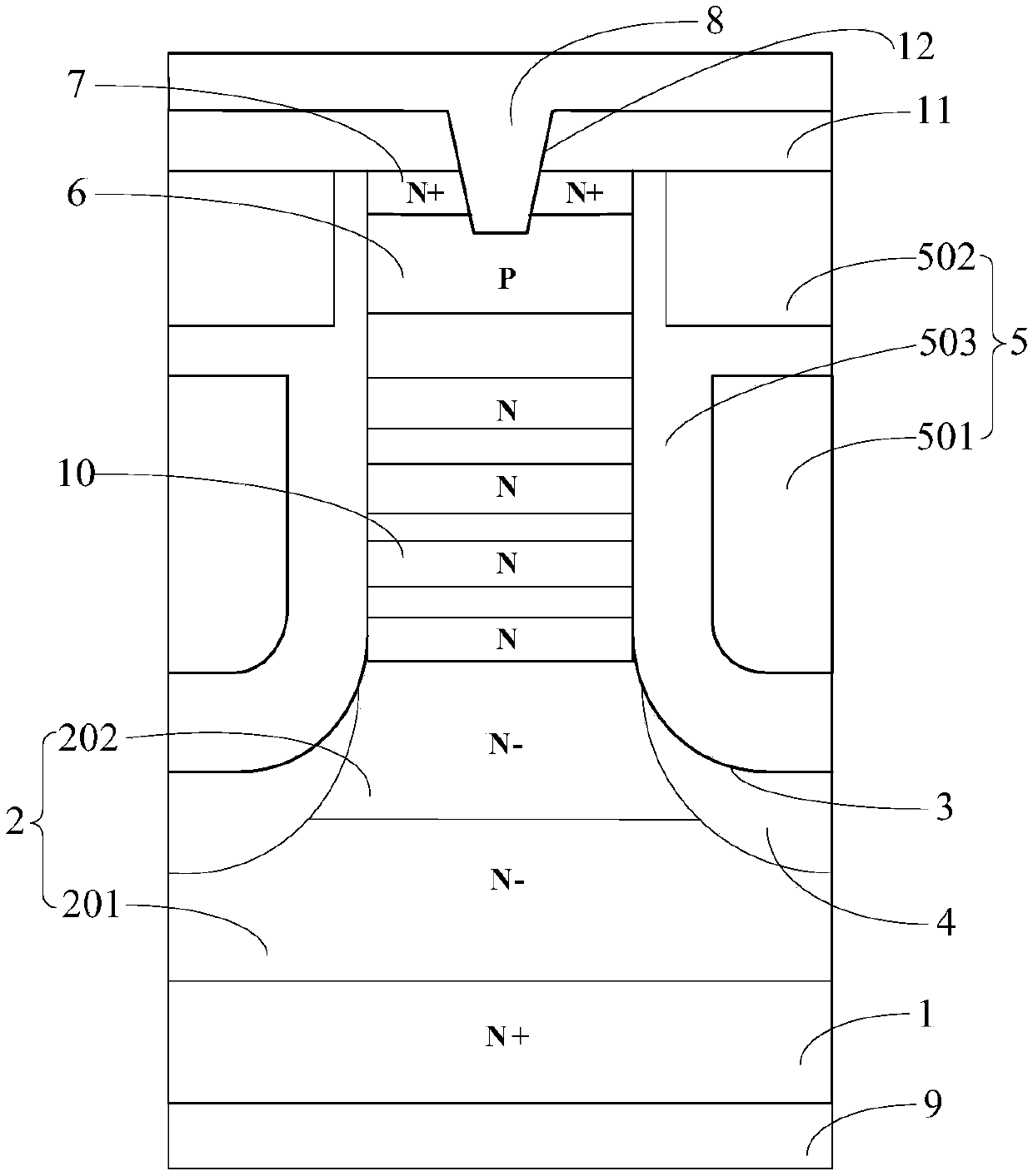
The invention provides a trench MOSFET and a manufacturing method thereof. The trench MOSFET comprises: a substrate having a first conductivity type; an epitaxial layer formed on the substrate and having a first conductivity type, the doping concentration of the epitaxial layer being lower than that of the substrate; a trench formed in the epitaxial layer; a buried layer formed below the trench and having a second conductivity type; a gate structure filled in the trench and comprising a shielding gate electrode, a control gate electrode positioned above the shielding gate electrode and a dielectric layer which covers the shielding gate electrode and is filled in the side part of the control gate electrode; a body region having a second conductivity type and formed in the epitaxial layer; and a source region formed in the epitaxial layer, positioned above the body region and having a first conductivity type, the doping concentration of the source region being greater than that of the body region.

Description

technical field [0001] The present application relates to the field of semiconductor technology, in particular to a trench MOSFET and a manufacturing method thereof. Background technique [0002] In the development of the semiconductor field, for medium and high voltage MOSFETs (Metal-Oxide-Semiconductor Field-Effect Transistors, Metal-Oxide-Semiconductor Field-Effect Transistors), improving the MOSFET's withstand voltage and reducing the specific on-resistance have become the focus of research. [0003] SGTMOS (Shielded Gate Trench MOS) includes a substrate, an epitaxial layer on the substrate, and a device structure within the epitaxial layer. The doping concentration of the epitaxial layer of the SGTMOS in the prior art is constant, and the withstand voltage of the SGTMOS can be improved by reducing the doping concentration of the epitaxial layer, but it will also cause the specific on-resistance of the SGTMOS (conduction per unit area On-resistance) rises. Therefore, t...

Claims


Application Information

Patent Timeline
Patent Type & Authority Applications(China)
IPC IPC(8): H01L29/78H01L29/423H01L29/06H01L21/336
CPCH01L29/7813H01L29/66484H01L29/66734H01L29/66787H01L29/4236H01L29/063H01L29/0634H01L29/0684
Inventor 张新李巍叶俊
Owner WUXI CHINA RESOURCES HUAJING MICROELECTRONICS
Learn More