Cesium lead halide perovskite thick film as well as preparation and application thereof

A cesium lead halide and perovskite technology, applied in the field of radiation detection, can solve the problems of inconsistent orientation, complex process, low sensitivity, etc., and achieve the effect of avoiding air holes

Active Publication Date: 2020-01-17
HUAZHONG UNIV OF SCI & TECH
View PDF8 Cites 3 Cited by
  • Summary
  • Abstract
  • Description
  • Claims
  • Application Information

AI Technical Summary

Problems solved by technology

[0004] In view of the above defects or improvement needs of the prior art, the object of the present invention is to provide a cesium lead halide perovskite thick film and its preparation and application, wherein through the overall process design (including temperature control program) of the preparation method, etc. Improvements can be made to obtain high-performance, consistent orientation, stable, high-sensitivity, and large-area quasi-single-crystal cesium lead halide perovskite thick films, and solve the problems of complex processes, low sensitivity, and inconsistent orientations in the prior art.

Method used


Image

  • Cesium lead halide perovskite thick film as well as preparation and application thereof
  • Cesium lead halide perovskite thick film as well as preparation and application thereof
  • Cesium lead halide perovskite thick film as well as preparation and application thereof

Examples


Embodiment example 1

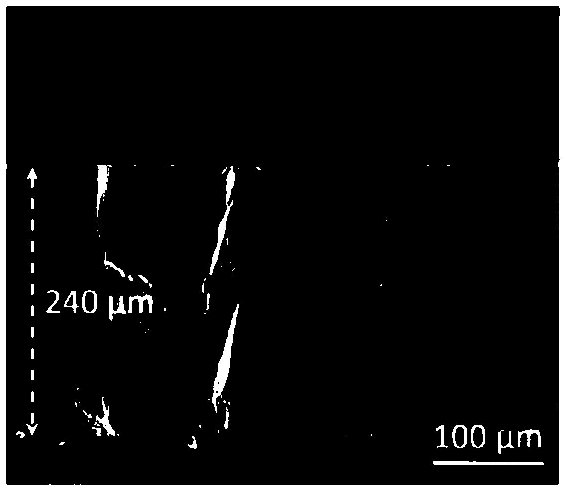
[0033] This example will introduce the preparation of 240um cesium lead bromide perovskite thick film on FTO substrate:

[0034] Take (0.5g) cesium lead bromide (CsPbBr 3 ) powder, spread the powder evenly on the FTO of 2.5cm×2.5cm, heat the FTO and powder to 600°C for 5min, cesium lead bromide (CsPbBr 3 ) powder melted into a liquid state, the quartz sheet heated in the same furnace was covered on the liquid cesium lead bromine, and then cooled to room temperature at a speed of 5°C / min, and then the quartz sheet was uncovered to obtain a cesium lead bromine thick film on the FTO substrate.

Embodiment example 2

[0036] This example will introduce the preparation of 480um cesium lead bromide perovskite thick film on FTO substrate:

[0037] Take (1g) cesium lead bromide (CsPbBr 3 ) powder, spread the powder evenly on the FTO of 2.5cm×2.5cm, heat the FTO and powder to 600°C for 5min, cesium lead bromide (CsPbBr 3 ) powder melted into a liquid state, the quartz was covered on the liquid cesium lead bromine, and then cooled to room temperature at a rate of 5°C / min, and then the quartz sheet was uncovered to obtain a cesium lead bromine thick film on the FTO substrate.

Embodiment example 3

[0039] This example will introduce the preparation of 240um cesium lead iodine perovskite thick film on FTO substrate:

[0040] Take (0.6g) cesium lead iodide (CsPbI 3 ) powder, spread the powder evenly on the FTO of 2.5cm×2.5cm, heat the FTO and powder to 570°C for 5min, cesium lead iodide (CsPbI 3) powder melted into a liquid state, the quartz was covered on the liquid cesium lead iodine, and then cooled to room temperature at a rate of 5°C / min, and then the quartz sheet was uncovered to obtain a cesium lead iodine thick film on the FTO substrate.


PUM

PropertyMeasurementUnit
surface roughnessaaaaaaaaaa

Abstract

The invention belongs to the technical field of radiation detection with preparation of semiconductor materials and discloses a cesium lead halide perovskite thick film as well as preparation and application thereof. The preparation method comprises the following steps: (1) dispersing a cesium lead halide perovskite material on a substrate, and performing heating to increase the temperature to being greater than the melting point of the cesium lead halide perovskite till the cesium lead halide perovskite is completely molten to a liquid state; (2) covering a perovskite material by quartz sheets, and uniformly dispersing the liquid perovskite material covered by the quartz sheets on the substrate; and (3) performing cooling by slowly reducing the temperature at a velocity of 0.1-5 DEG C/min, and peeling off the quartz sheets, so as to obtain the perovskite thick film adhered to the substrate. Due to improvement of overall process procedure designing (including temperature control procedures) and the like of the preparation method, a thick film with good performance, consistent orientation, stability, high sensitivity and large areas can be prepared, and the problems that in the prior art, the process is complex, the sensitivity is low, the orientation is inconsistent, and the like, can be solved.

Description

technical field [0001] The invention belongs to the technical field of radiation detection prepared by semiconductor materials, and more specifically relates to a cesium lead halide perovskite thick film and its preparation and application, wherein the quasi-single crystal cesium lead halide perovskite thick film obtained by the preparation method is Films can be used in particular as functional materials in radiation detectors. Background technique [0002] Radiation imaging detectors are widely used in industries such as healthcare, public safety and high-end manufacturing. Detectors used to detect radioactive rays generally include gas detectors, scintillation detectors, semiconductor detectors, etc., among which semiconductor detectors can obtain the best energy resolution. Since the X-ray refractive index is 1, it is difficult to focus X-rays, so a large-area semiconductor thick film matching the imaging size is required. [0003] In recent years, organic-inorganic hy...

Claims


Application Information

Patent Timeline
Patent Type & Authority Applications(China)
IPC IPC(8): C03C17/22C04B41/85H01L31/032H01L31/0392H01L31/115
CPCC03C17/22C03C2217/284C03C2218/13C04B41/009C04B41/5011C04B41/85H01L31/032H01L31/0392H01L31/115C04B35/583C04B41/4523
Inventor 牛广达唐江潘伟程杨波
Owner HUAZHONG UNIV OF SCI & TECH
Why Eureka
Try Eureka