Sample sealing and vacuum transferring device for cross-platform connection

A transfer device and cross-platform technology, applied to measurement devices, material analysis using wave/particle radiation, instruments, etc., can solve problems such as time-consuming, randomness in the selection and analysis of samples to be observed, and inaccurate analysis results

Pending Publication Date: 2020-01-24
INST OF METAL RESEARCH - CHINESE ACAD OF SCI
View PDF0 Cites 10 Cited by
  • Summary
  • Abstract
  • Description
  • Claims
  • Application Information

AI Technical Summary

Problems solved by technology

[0003] Scanning electron microscope, double-beam electron microscope and micro-nano laser processing system have been widely used in traditional materials, advanced new materials, semiconductor materials, nanotechnology and catalytic materials, realizing magnetic materials, low dielectric coefficient materials, biological / medical materials Direct fine processing and high-resolution characterization of polymer composites and ceramic materials have shown great potential in the fields of new materials, environment, energy and chemistry, but there are still problems of sample transfer, pollution and oxidation
[0004] The main problem of the prior art is that the commonly used sample processing methods for energy materials are likely to cause the sample to be polluted or mechanically damaged by water, oxygen, processing liquid, etc.
Therefore, there are many interference factors in the micro-analysis of microscopic morphology, organizational structure and composition, resulting in a series of problems such as low success rate of sample preparation and inaccurate analysis results, which is difficult to meet the requirements of research work. For samples to be observed There is also a lot of randomness in the selection and analysis of
Because the sample transfer process is not only complicated and time-consuming, but also there is a great risk of damage and recontamination during sample transfer, processing, and switching between different electron microscopes and processing platforms

Method used


Image

  • Sample sealing and vacuum transferring device for cross-platform connection
  • Sample sealing and vacuum transferring device for cross-platform connection

Examples


Embodiment Construction

[0028] The specific implementation manner of the invention will be described in further detail below in conjunction with the accompanying drawings and embodiments. For the detailed description of these embodiments, it should be understood that those skilled in the art can practice the present invention, and can use other embodiments without departing from the spirit of the appended claims and the scope of the present invention. Modifications and / or changes are made to the examples shown. Furthermore, although specific features of the present invention have been disclosed in the embodiments, such specific features can be properly modified to achieve the functions of the present invention.

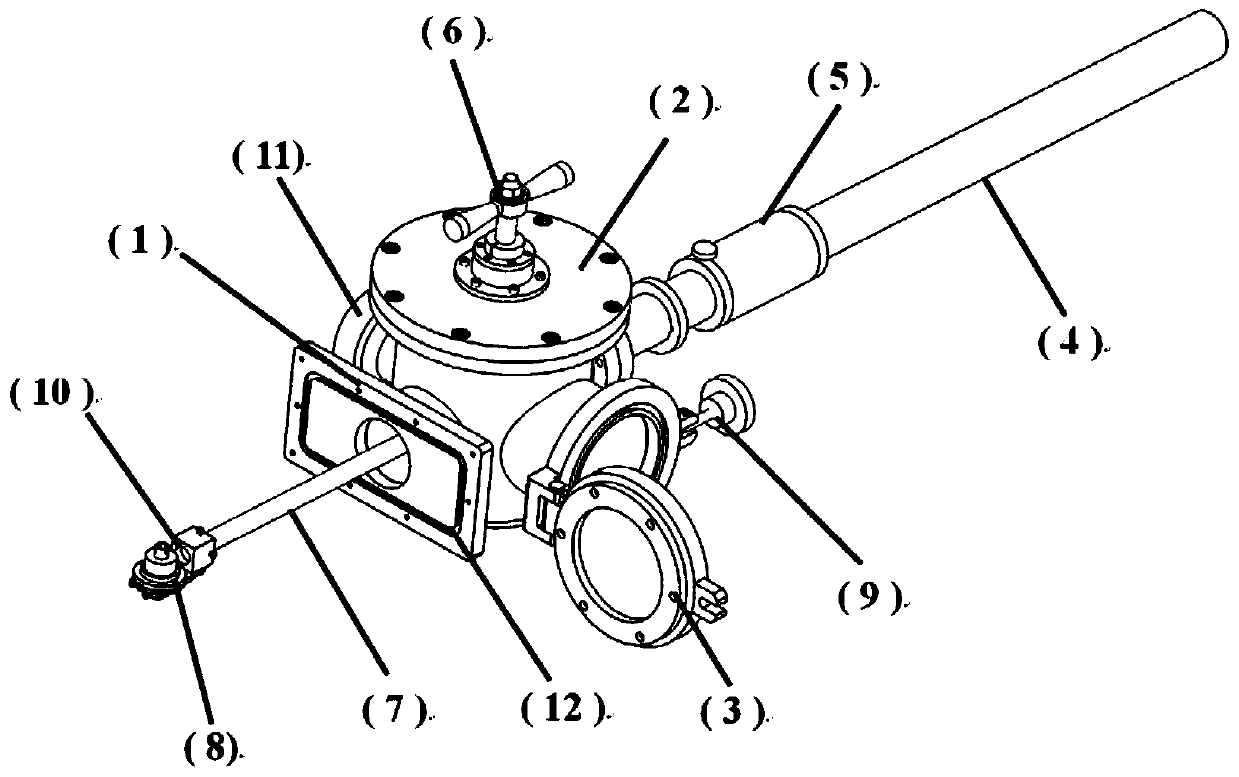
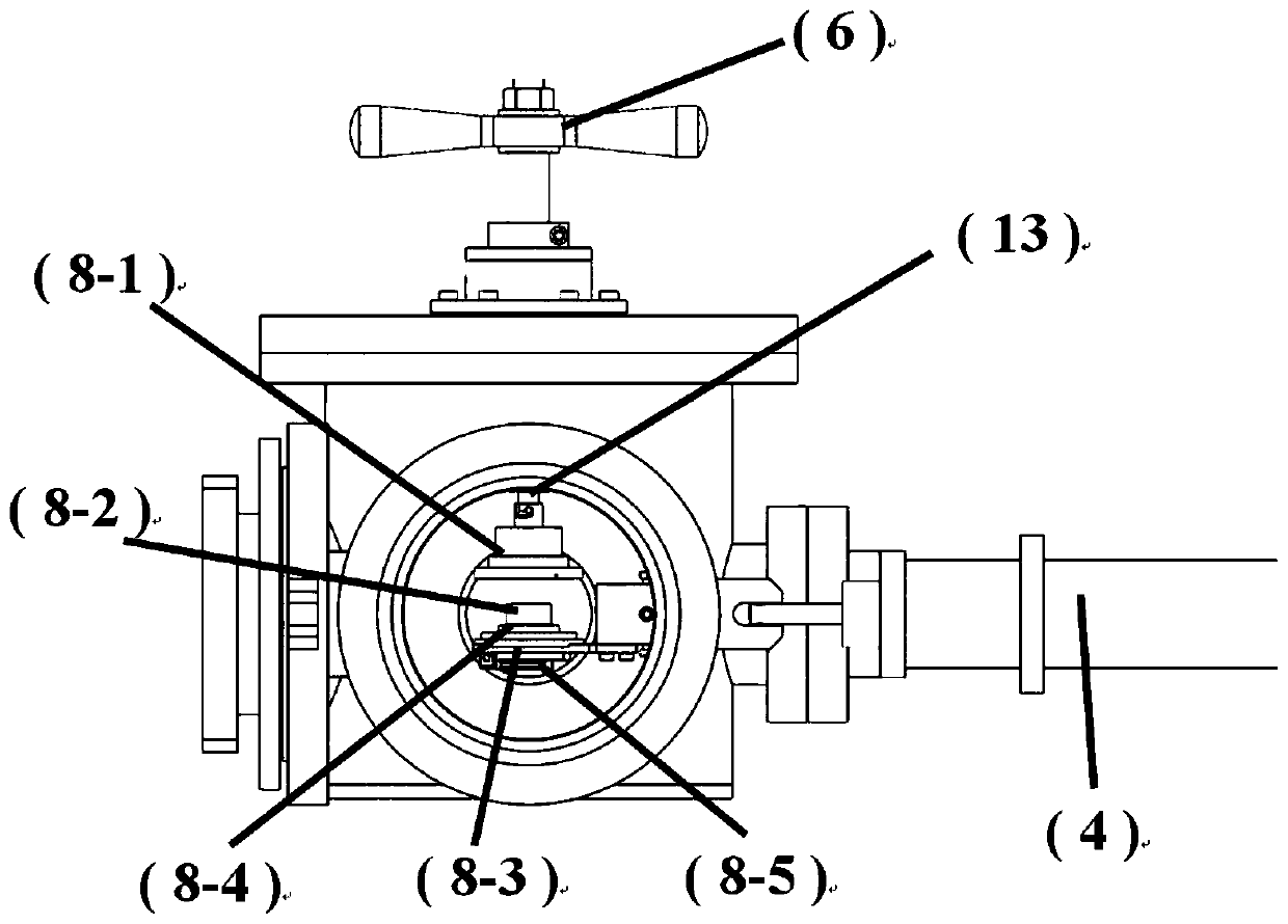
[0029] Such as Figure 1-Figure 2As shown, the sample sealing and vacuum transfer device for the cross-platform connection of electron microscope or micro-nano laser processing system of the present invention mainly includes: a vacuum sample chamber and a vacuum transition chamber for conne...


PUM


Abstract

The invention relates to the technical field of material testing, and specifically relates to a sample sealing and vacuum transferring device for cross-platform connection of an electron microscope ora micro-nano laser processing system. The device comprises a rectangular airtight flange, a vacuum sealing transferring box, a high-precision support, a clamp structure, a mechanical arm unlocking mechanism, a vacuum transition bin, an observation window and a bin door, wherein the rectangular airtight flange is used for being connected with the side wall of an electron microscope vacuum sample chamber or a laser processing system vacuum cavity; the vacuum sealing transferring box is used for packaging a test sample; the high-precision support and the clamp structure are used for achieving connection of the sample and the electron microscope or the micro-nano laser processing system; the mechanical arm unlocking mechanism is used for controlling the vacuum sealing transferring box; the vacuum transition bin is used for placing and replacing the vacuum sealing transferring box; the observation window is used for determining the opening state of the vacuum sealing transferring box; andthe bin door is used for observing opening. The sample sealing and vacuum transferring device can be widely applied to cross-platform connection and vacuum transferring of scanning electron microscopes, electron beam and ion beam double-beam electron microscopes or micro-nano laser processing systems of various types, and a systematic sample assembling, protecting, transferring and feeding deviceis formed.

Description

technical field [0001] The invention relates to material testing technology, specifically a sample sealing and vacuum transfer device used for cross-platform connection of glove boxes, scanning electron microscopes, double-beam electron microscopes or micro-nano laser processing systems, belonging to electron microscope or micro-nano laser processing system accessories and The field of material microstructure testing and analysis. Background technique [0002] Double-beam electron microscope and micro-nano laser processing system are important tools for high-precision processing, modification, and molding of nano- and micro-scale structures of materials. Using the focused ion beam processing function equipped with double-beam electron microscopes, continuous high-precision preparation and molding of structures from the scale of nearly 10nm to microns can be achieved. Using scanning electron microscopy and electron beam high-resolution microscopic characterization methods in...

Claims


Application Information

Patent Timeline
Patent Type & Authority Applications(China)
IPC IPC(8): G01N23/2204G01N23/2202G01N23/2005G01N23/20025
CPCG01N23/20025G01N23/2005G01N23/2202G01N23/2204
Inventor 谭军唐培李峰
Owner INST OF METAL RESEARCH - CHINESE ACAD OF SCI
Why Eureka
Try Eureka