PNP BJT combined capacitor charge-discharge controller with wide operating voltage range
A technology of working voltage range and combined capacitance, applied in control/regulation systems, instruments, electrical components, etc., can solve the problems of miniaturization and high efficiency of converters, occupying space, increasing losses, etc.
- Summary
- Abstract
- Description
- Claims
- Application Information
AI Technical Summary
Problems solved by technology
Method used
Image

Examples
Embodiment 1
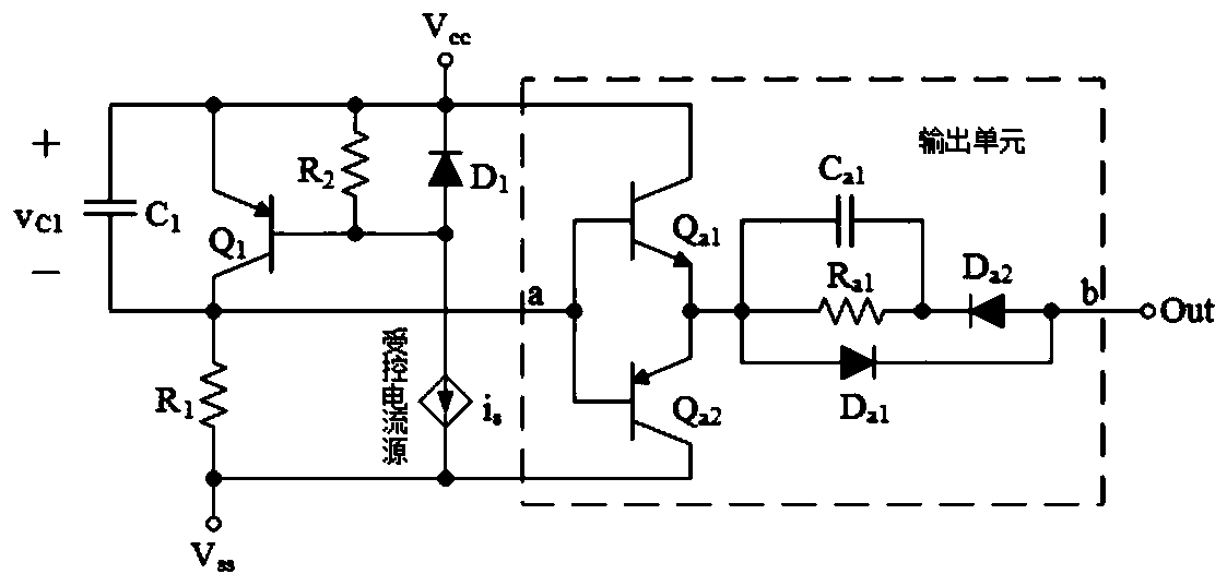
[0044] refer to figure 1 and Figure 4 , a PNP BJT combined capacitor charging and discharging controller with a wide operating voltage range, including the port V cc , port V ss and port Out, also includes PNP type BJT tube Q 1 , Diode D 1 , capacitance C 1 , resistance R 1 , resistance R 2 , controlled current source and output unit, the output unit includes port a and port b, PNP type BJT tube Q 1 the emitter simultaneously with the resistor R 2 One end of the capacitor C 1 One end of the diode D 1 the cathode and the port V cc Connected, PNP type BJT tube Q 1 base simultaneously with resistor R 2 The other end of the diode D 1 The anode and the first port of the controlled current source are connected, and the PNP type BJT tube Q 1 collector simultaneously with capacitor C 1 The other end of the resistor R 1 One end of the output unit is connected to the port a of the output unit, the port b of the output unit is connected to the port Out, and the resistanc...
Embodiment 2
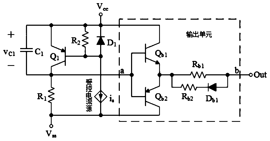
[0056] refer to figure 2 and Figure 4 , a PNP BJT combined capacitor charging and discharging controller with a wide operating voltage range, its output unit includes an NPN type BJT tube Q b1 , PNP type BJT tube Q b2 , resistance R b1 , resistance R b2 and diode D b1 , NPN type BJT tube Q b1 collector with port V cc Connected, NPN type BJT tube Q b1 The base of the output unit is simultaneously connected with the port a of the output unit and the PNP type BJT tube Q b2 The base is connected, PNP type BJT tube Q b2 collector with port V ss Connected, NPN type BJT tube Q b1 The emitter of the PNP type BJT tube Q b2 The emitter, resistor R b1 One end of the resistor R b2 Connected to one end of the resistor R b2 The other end of the diode D b1 connected to the cathode of the diode D b1 The anode of the resistor Rb1 is connected to the other end of the resistor Rb1 and port b at the same time.
[0057] The rest of embodiment 2 is the same as embodiment 1.
[0...
Embodiment 3
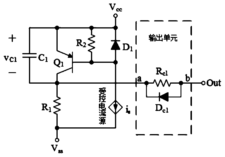
[0066] refer to image 3 and Figure 4 , a PNP BJT combined capacitor charging and discharging controller with a wide operating voltage range, its output unit includes a resistor R c1 and diode D c1 , resistor R c1One end of the diode D c1 The cathode is connected to port a, the resistor R c1 The other end of the diode D c1 The anode is connected to port b.
[0067] The rest of the embodiment 3 is the same as the embodiment 2, but the driving ability is weaker than that of the embodiment 2.
[0068] refer to Figure 11 , applying the controller to a step-down converter. In addition to the controller, the converter also includes an inductor L k1 , Diode D k5 , capacitance C k1 , Diode D k1 , Diode D k2 , PNP type BJT tube Q k1 , resistance R k1 , Diode D k3 , PNP type BJT tube Q k2 , resistance R k2 , Diode D k4 , inductance L k2 , capacitance C k2 , resistance R k3 , resistance R k4 and capacitance C k3 , the positive terminal of the DC power supply is ...
PUM
 Abstract
Description
Claims
Application Information