Variable-component variable-doping reflective Al<x>Ga<1-x>As/GaAs photocathode and preparation method thereof
A photocathode and variable doping technology, which is used in the manufacture of light-emitting cathodes, image conversion/image amplifier tubes, cathode ray tubes/electron beam tubes, etc. Efficiency, the effect of improving transport capacity
- Summary
- Abstract
- Description
- Claims
- Application Information
AI Technical Summary
Problems solved by technology
Method used
Image
Examples
preparation example Construction
[0035] A variable composition variable doping reflective Al x Ga 1-x The preparation method of As / GaAs photocathode comprises the following steps:
[0036] Step 1: growing a GaAs transition layer on the GaAs substrate.
[0037] Step 2: Then grow Al composition Al on the GaAs transition layer x Ga 1-x As buffer layer.
[0038] Step 3: Change Al composition Al x Ga 1-x The As buffer layer is sequentially grown into individual unit layers of the exponentially doped GaAs emitter layer.
[0039] Step 4: Chemically clean the surface of the variable-composition variable-doped GaAs photocathode generated in step 3, and then send it to an ultra-high vacuum system for high-temperature heating, so that the surface of the GaAs photocathode is clean at the atomic level.
[0040] Step 5: Through the ultra-high vacuum activation process, the Cs and O 2 The alternating adsorption of Cs / O active layer is formed, and the high quantum efficiency variable composition variable doping refle...
specific Embodiment
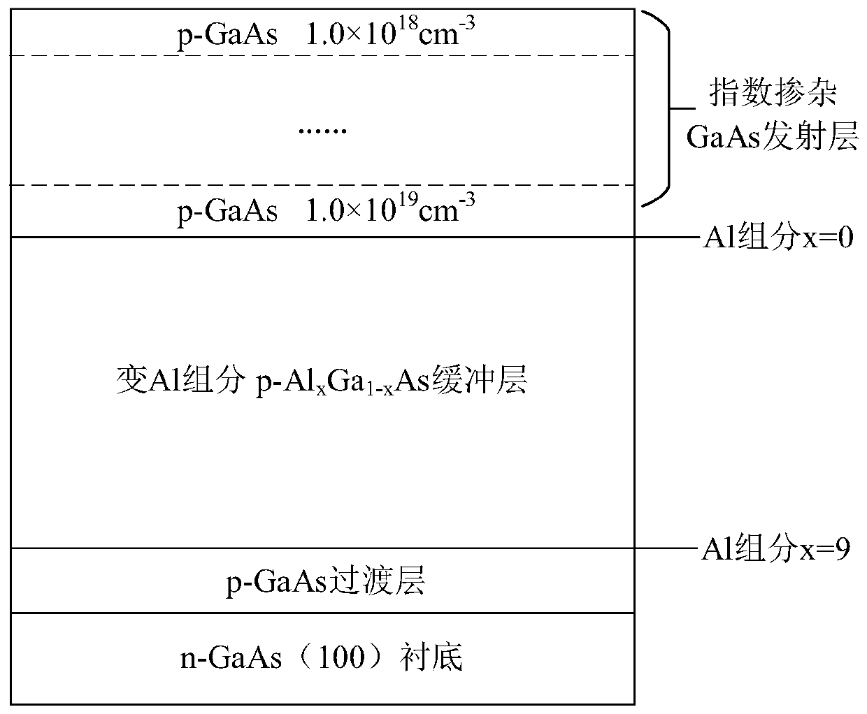
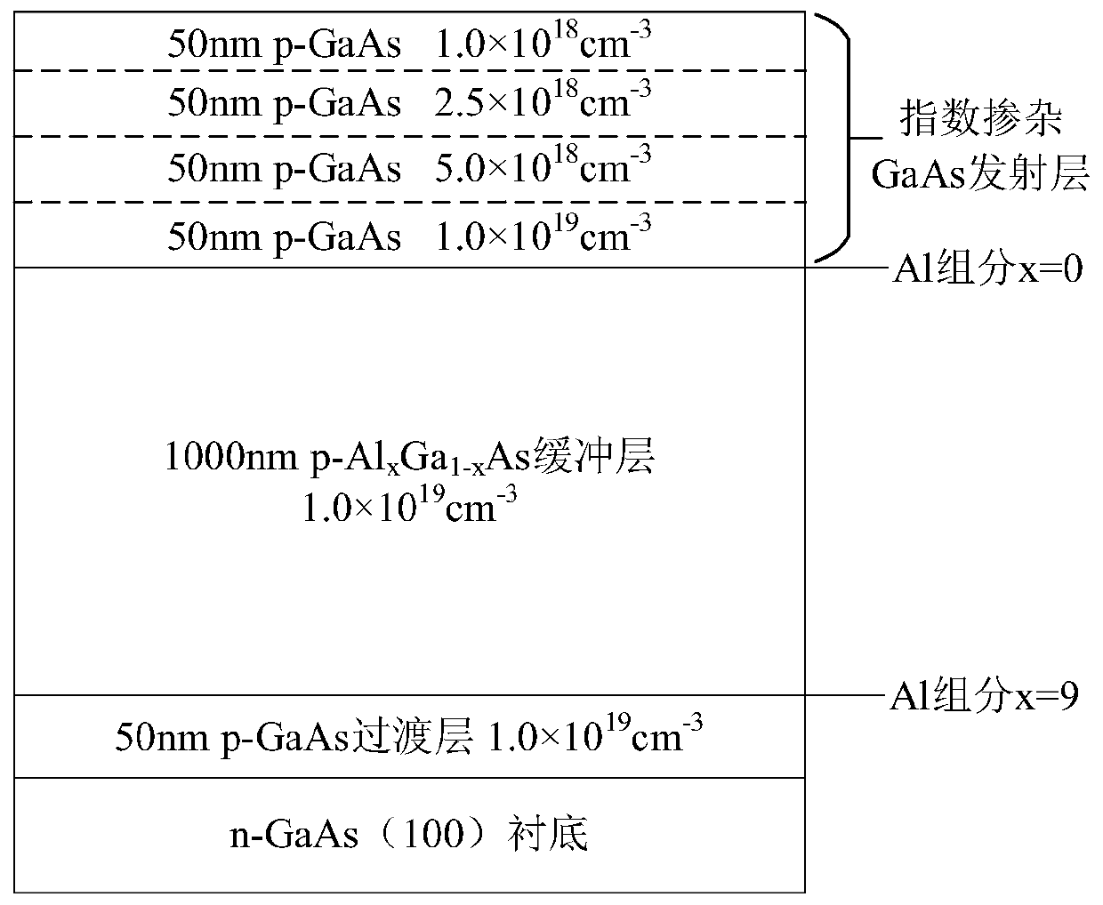
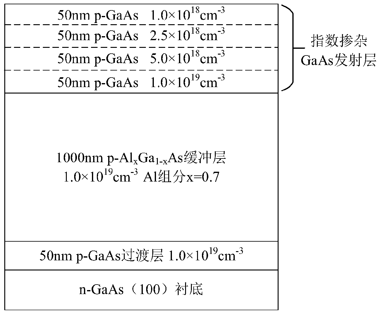
[0044] Such as figure 2 As shown, the variable composition variable doping reflective Al made by the method of the present invention x Ga 1-x Schematic diagram of the As / GaAs photocathode structure. The cathode consists of a p-type GaAs transition layer with a thickness of 50nm from bottom to top, and a doping concentration of 1.0×10 19 cm -3 ; Thickness of 1000nm p-type variable Al component Al x Ga 1-x As buffer layer, the doping concentration is 1.0×10 19 cm -3 , the Al composition gradually changes from 0.9 to 0 from the rear interface to the emission layer interface; and the p-type index-doped GaAs emission layer with a total thickness of 200nm, the emission layer is a layered structure of 4 units, and the thickness of each unit is 50nm, the doping concentration from the rear interface to the emission surface is 1.0×10 19 cm -3 , 5.0×10 18 cm -3 , 2.5×10 18 cm -3 , 1.0×10 18 cm -3 .
[0045] The variable composition variable doping reflective Al x Ga 1-...
PUM
| Property | Measurement | Unit |
|---|---|---|
| thickness | aaaaa | aaaaa |
| thickness | aaaaa | aaaaa |
| thickness | aaaaa | aaaaa |
Abstract
Description
Claims
Application Information


