Gate structure applied to crimping MOSFET

A gate structure, crimping technology, applied in electrical components, electrical solid devices, circuits, etc., can solve problems such as pressure differences, and achieve the effect of simple structure and reliable connection

Pending Publication Date: 2020-02-07
TSINGHUA UNIV
View PDF0 Cites 1 Cited by
  • Summary
  • Abstract
  • Description
  • Claims
  • Application Information

AI Technical Summary

Problems solved by technology

However, the introduction of multi-layer circuit boards will have a barrier effect on the process of MOSFET transferring heat to the outside world.
[0007] In addition, when using GCT or GTO, it is necessary to crimp the molybdenum sheet on both sides, and apply a pressure of more than tens of KN, and a single crimping MOSFET can only withstand the pressure of 50-100N. Therefore, if the crimping type MOSFET is integrated in the shell, there are pressure differences and coordination problems of different components

Method used


Image

  • Gate structure applied to crimping MOSFET
  • Gate structure applied to crimping MOSFET
  • Gate structure applied to crimping MOSFET

Examples


Embodiment Construction

[0042] The present invention will be described in detail below in conjunction with the accompanying drawings and specific embodiments, but not as a limitation of the present invention.

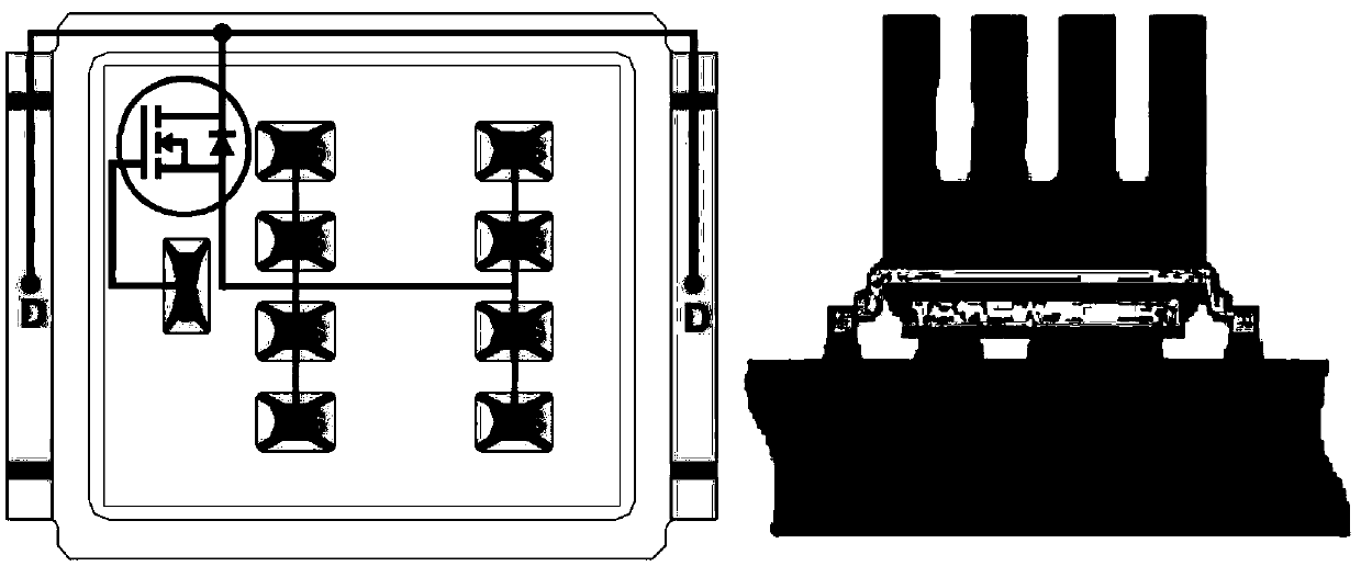
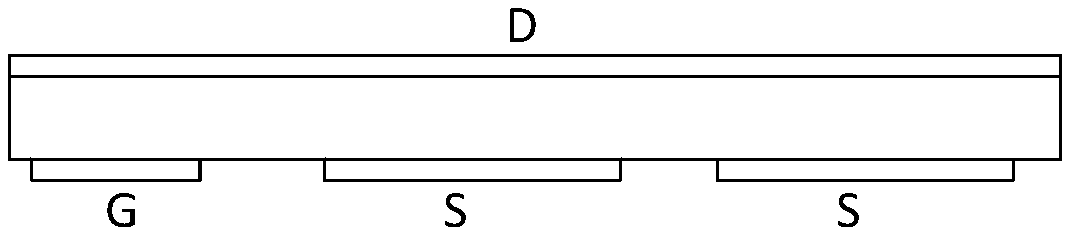
[0043] In one embodiment, the press-fit overall structure of a press-fit MOSFET with a gate structure is as follows Figure 4As shown, it includes a first copper block 41, a crimping type MOSFET 42, a gate connector 43, a connection interface 44 for receiving external gate control signals, a second copper block 45, an elastic structure 46, and the crimping type MOSFET 42 gate The rod-shaped metal 47 in pole contact, the insulating medium 48 between the gate connecting piece 43 and the second copper block 45; wherein, the gate connecting piece 43 can be in the shape of a gate ring or a grid.

[0044] Wherein, the first copper block 41 is at the same potential as the drain of the pressure-contact MOSFET 42 , and the second copper block 45 is at the same potential as the source of the pressure-co...


PUM


Abstract

A gate structure applied to a crimping MOSFET comprises a first copper block, the crimping MOSFET, a gate connecting piece, a connection interface for receiving an outer gate control signal, a secondcopper block, rod-like metal in contact with a gate of the crimping MOSFET, an elastic structure used for connection between the rod-like metal and the gate connecting piece, and an insulating mediumbetween the gate connecting piece and the second copper block. The gate structure having no obstruction function on a MOSFET cooling path is used, so that a heat dissipation capability can be improved, and at the same time, a press fitting structure is simplified.

Description

technical field [0001] The invention relates to a gate structure of a MOSFET, in particular to a gate structure applied to a crimping MOSFET or a crimping MOSFET array, and belongs to the technical field of electrical engineering. Background technique [0002] Metal-Oxide Semiconductor Field-Effect Transistor, abbreviated as Metal-Oxide-Semiconductor Field-Effect Transistor (MOSFET), is a field-effect transistor that can be widely used, and it can be applied to such as microprocessors, In the case of digital signal processing such as microcontrollers, more and more integrated circuits for analog signal processing are implemented with MOSFETs. [0003] The traditional MOSFET has a lateral flow structure, and its gate, drain, and source are usually welded on the circuit board. The heat generated by the device is mainly dissipated through the circuit board. Affected by the package type, the heat dissipation capability is poor. limited its flow capacity. Press-fit MOSFETs, suc...

Claims


Application Information

Patent Timeline
Patent Type & Authority Applications(China)
IPC IPC(8): H01L25/07H01L23/48
CPCH01L24/72H01L25/072H01L2224/16225H01L2224/73253
Inventor 陈政宇曾嵘赵彪余占清刘佳鹏周文鹏
Owner TSINGHUA UNIV
Why Eureka
Try Eureka