Electrical device

A technology for electrical devices and components, applied in the field of electronic circuits, can solve the problems of complex packaging structure and pressure difference, and achieve the effects of reducing production cost, simple structure, and increasing flow capacity.

Pending Publication Date: 2020-02-07
TSINGHUA UNIV
View PDF0 Cites 1 Cited by
  • Summary
  • Abstract
  • Description
  • Claims
  • Application Information

AI Technical Summary

Problems solved by technology

[0003] For power semiconductor devices in the prior art, power semiconductor elements (sometimes also called device wafers, device chips or device dies) and shutdown modules are generally placed in packages (also called tube shells), and the power semiconductor element gates The inner and outer sides of the pole ring are cathodes, and the conductive blocks used to connect the cathodes need to isolate multiple channels for connecting the gates, that is, multiple cathode conductive blocks are required, so the packaging structure is more complicated.
[0004] In addition, when using GCT or GTO, molybdenum sheets need to be crimped on both sides, and a pressure of tens of Newtons or more must be applied when crimping the molybdenum sheets, and the pressure on the switching elements in the drive module may be enormous during this process. Due to the pressure it can withstand, a single switch element can only withstand a pressure of 50-100N. Therefore, if the switch element is integrated in the shell, there will be pressure differences and coordination problems between different components

Method used


Image

  • Electrical device
  • Electrical device
  • Electrical device

Examples


Embodiment Construction

[0048] In order to make the purpose, technical solutions and advantages of the embodiments of the present invention more clear, the technical solutions in the embodiments of the present invention will be clearly and completely described below in conjunction with the accompanying drawings in the embodiments of the present invention. Obviously, the described embodiments It is a part of embodiments of the present invention, but not all embodiments. Based on the embodiments of the present invention, all other embodiments obtained by persons of ordinary skill in the art without making creative efforts belong to the protection scope of the present invention.

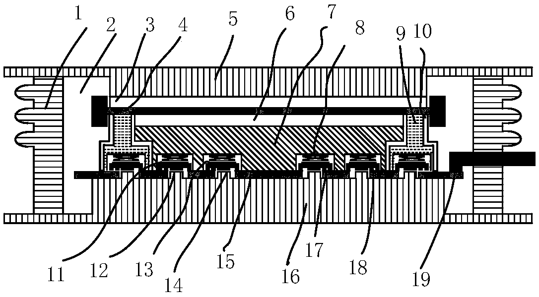
[0049] Such as figure 1 As shown, the embodiment of the present invention introduces a schematic structural diagram of an electrical device, figure 1The electrical device described in includes a third conductive block 5 , a power semiconductor element 4 , a first conductive block 7 , a connector 9 , an elastic structure 8 , a...


PUM


Abstract

The invention discloses an electrical device. The electrical device comprises a power semiconductor element, a driving module, one or more first conductive blocks and one or more elastic structures, wherein a control electrode and a current electrode of the power semiconductor element are annularly arranged, the control electrode is arranged on the annular outer ring, and the current electrode isarranged on the inner ring; the driving module comprises one or more switch elements, and is used for driving the power semiconductor element; the one or more first conductive blocks are arranged on one side of the power semiconductor element, and are used for providing connection from the switch elements to the current electrode; and the elastic structures comprise bases, auxiliary elastic piecesand springs. The electrical device has the characteristics of small commutation circuit area, low commutation circuit stray inductance and high commutation speed, the elastic structures in the electrical device provide pressure for the contact surface between the conductive blocks and a circuit board, the contact resistance is decreased, and the upper limit of the pressure borne by the surfaces of the switch elements can be limited.

Description

technical field [0001] The invention belongs to the technical field of electronic circuits, and in particular relates to an electrical device. Background technique [0002] In the face of the rapid development of power electronics technology, users put forward requirements for power semiconductor devices (here also referred to as semiconductor devices or power devices) for fast commutation speed during turn-off period, high turn-off reliability, and good heat dissipation performance. The package structure of a power semiconductor device is particularly critical for a good electrical connection between the semiconductor device and an external circuit, especially for a power semiconductor device suitable for a high-voltage and high-current environment. [0003] For power semiconductor devices in the prior art, power semiconductor elements (sometimes also called device wafers, device chips or device dies) and shutdown modules are generally placed in packages (also called tube s...

Claims


Application Information

Patent Timeline
Patent Type & Authority Applications(China)
IPC IPC(8): H01L25/16H01L23/48H01L23/367H01L23/473
CPCH01L23/367H01L23/473H01L23/48H01L25/16
Inventor 曾嵘陈政宇赵彪余占清刘佳鹏周文鹏
Owner TSINGHUA UNIV
Why Eureka
Try Eureka