
Timing controller for dead-time control

A timing control and control circuit technology, which is applied in the direction of control/regulation systems, conversion equipment and instruments without intermediate conversion to AC, and can solve the problems of reduced benefits of GaN devices

Pending Publication Date: 2020-02-07
PSEMI CORP
View PDF6 Cites 4 Cited by
  • Summary
  • Abstract
  • Description
  • Claims
  • Application Information

AI Technical Summary

Problems solved by technology

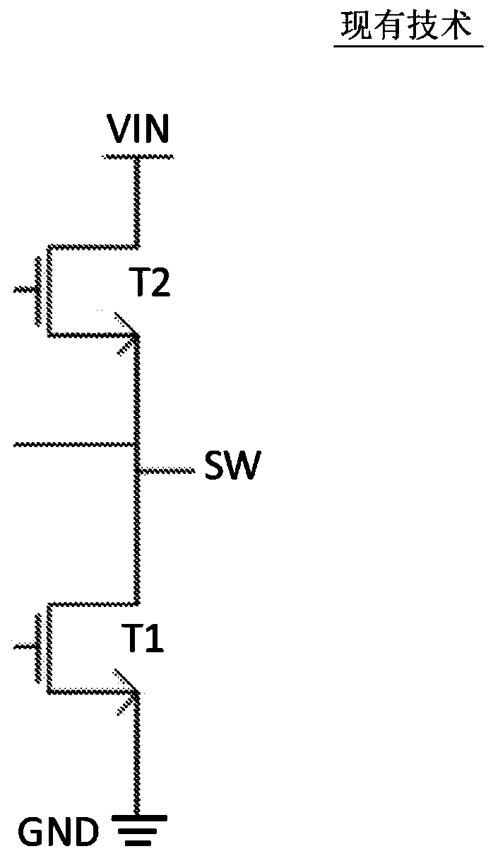
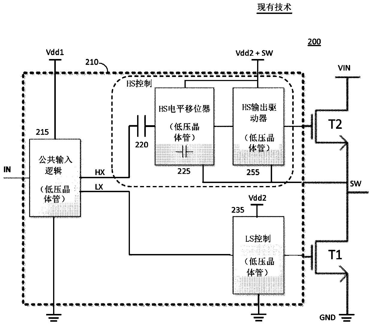
Since these control transistors typically have a poor FOM compared to the figure of merit (FOM) of the GaN device, which may, for example, limit the operating frequency of the GaN device, the overall circuit (e.g., power management) may be dominated by large high voltages in performance Transistors - which may be difficult to charge and discharge quickly (eg their FOM is too high) - are limited and thus the benefit of using GaN devices may be significantly reduced

Method used


Image

  • Timing controller for dead-time control
  • Timing controller for dead-time control
  • Timing controller for dead-time control

Examples


Embodiment Construction

[0043] As used in this disclosure, the figure of merit (FOM) of a switching transistor (e.g., a transistor that can have a conducting ON state and a non-conducting OFF state)—also simply referred to as FOM—refers to the ON (conducting pass) resistance R on and transistor gate charge Q g product of . A lower FOM may indicate higher switching performance of the transistor. Having a low FOM—especially at high withstand voltages—is a unique characteristic of GaN transistors, which can handle up to 100 volts at a FOM that is about one-tenth that of a high-voltage MOSFET.

[0044] As used in this disclosure, a low-voltage device or low-voltage transistor refers to a semiconductor transistor device with a low breakdown voltage that can withstand and block (e.g., in the OFF state) less than 10 volts and more typically significantly less than 10 volts A DC voltage (eg, less than 3.3 volts to 5 volts) (typically applied between the source and drain terminals of a transistor, or betwe...


PUM

PropertyMeasurementUnit
Thicknessaaaaaaaaaa
Thicknessaaaaaaaaaa

Abstract

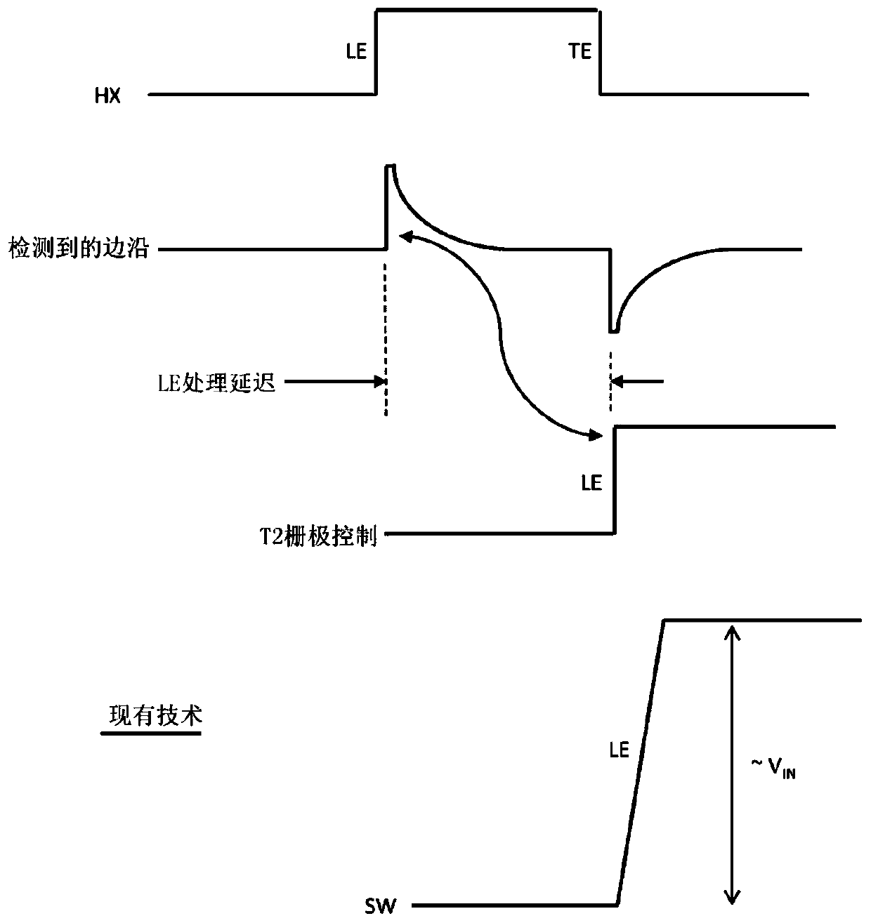
Systems, methods, and apparatus for use in biasing and driving high voltage semiconductor devices (T1, T2) using only low voltage transistors (inside 410) are described. The apparatus (410) and methodare adapted to control multiple high voltage semiconductor devices (T1, T2) to enable high voltage power control, such as power amplifiers, power management and conversion (e.g. DC / DC) and other applications wherein a first voltage (Vin) is large compared to the maximum voltage handling of the low voltage control transistors (Vdd1, Vdd2). According to an aspect, timing control of edges (fig. 4: 215, fig.14a: 1410 ) of a control signal (IN) to the high voltage semiconductor devices (T1, T2) is provided by a basic edge delay circuit (fig. 4: inside 215, fig. 14a: 1410) that includes a transistor, a current source and a capacitor. An inverter can be selectively coupled, via a switch, to an input and / or an output of the basic edge delay circuit to allow for timing control of a rising edge ora falling edge of the control signal.

Description

[0001] Cross References to Related Applications [0002] This application claims priority to US Patent Application 15 / 627,196, filed June 19, 2017, entitled "DC-Coupled High-Voltage LevelShifter," the entire disclosure of which is incorporated herein by reference. [0003] This application may be related to US Patent No. 9,484,897, issued November 1, 2016, entitled "Level Shifter," the entire disclosure of which is incorporated herein by reference. This application may be related to US Patent No. 5,416,043, issued May 6, 1995, entitled "Minimum charge FET fabricated on an ultrathin silicon on sapphire wafer," the entire disclosure of which is incorporated herein by reference. This application may also be related to US Patent No. 5,600,169, issued February 4, 1997, entitled "Minimum charge FET fabricated on an ultrathin siliconon sapphire wafer," the entire disclosure of which is incorporated herein by reference. This application may also be related to US Patent Application Seri...

Claims


Application Information

Patent Timeline
IPC IPC(8): H03K17/687H03K5/003H01L27/088H01L27/12H02M3/07H02M3/158H03K19/0175H03K17/10H03K5/1534H03K5/00
CPCH03K5/003H03K17/687H03K5/1534H03K2005/00293H02M1/08H03K19/018507H01L27/0928H03K17/102H01L21/84H01L21/86H03K19/017509H02M3/07H02M3/158H01L27/088H01L27/1203
Inventor 布迪卡·阿贝辛哈默林·格林加里·春贤·吴
Owner PSEMI CORP
Learn More