Method for growing patterned GaN on sapphire template and GaN epitaxial wafer

A patterning and sapphire technology, applied in the direction of gaseous chemical plating, coating, metal material coating process, etc., can solve the problem that etching damage cannot be completely avoided

Inactive Publication Date: 2020-02-11
SUN YAT SEN UNIV
View PDF5 Cites 7 Cited by
  • Summary
  • Abstract
  • Description
  • Claims
  • Application Information

AI Technical Summary

Problems solved by technology

However, improving the etching result by changing the gas involved in the etching can only reduce the etching damage to a certain extent, and cannot completely avoid the etching damage.

Method used


Image

  • Method for growing patterned GaN on sapphire template and GaN epitaxial wafer
  • Method for growing patterned GaN on sapphire template and GaN epitaxial wafer
  • Method for growing patterned GaN on sapphire template and GaN epitaxial wafer

Examples


Embodiment 1

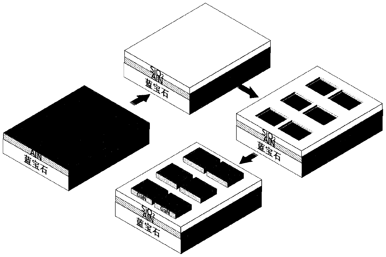
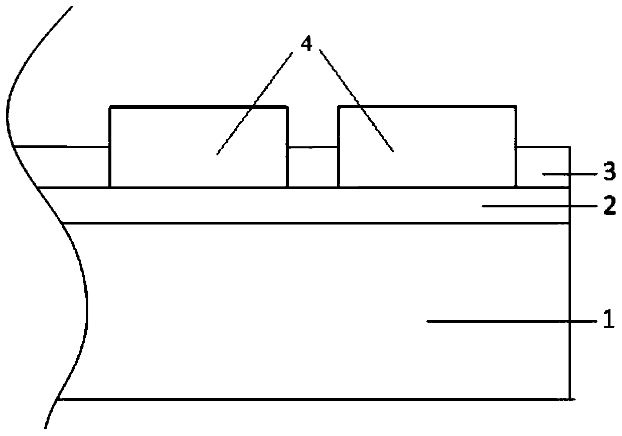
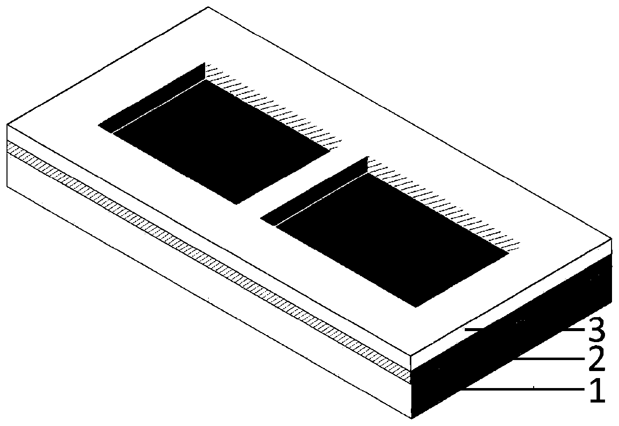
[0041] In this example, the GaN epitaxial wafer required in a terahertz Schottky diode (where the GaN mesa is composed of two 60μm×60μm square raised GaN modules) is taken as an example, and a patterned GaN layer is grown on a sapphire template. The target device The profile of figure 2 As shown, the patterned GaN is specifically two square bump modules, figure 2 Middle: 1 is sapphire substrate, 2 is AlN nucleation layer, 3 is SiO 2 Dielectric layer 4 is a patterned GaN layer.

[0042] Specific steps are as follows:

[0043] (1) Growth of AlN nucleation layer 2 on sapphire substrate 1: place the cleaned sapphire substrate in an MOCVD reaction chamber, and grow a 100nm AlN nucleation layer at 800°C, the Al source and N The source consists of TMAl and NH respectively 3 supply;

[0044] (2) Growth of SiO on the AlN nucleation layer 2 2 Medium layer 3. The cleaned sample (sapphire substrate with AlN nucleation layer grown) was placed in the PECVD reaction chamber and depo...

Embodiment 2

[0050] Other conditions are consistent with embodiment 1, only with SiO 2 The thickness of the dielectric layer is changed to 200nm, and the temperature of the secondary epitaxial growth of GaN is changed to 1100°C.

[0051] Observing the GaN epitaxial wafer obtained after the growth is completed, it can be seen that the side wall of the GaN mesa is smooth, the edge is flat, there is no etching damage, and the mask part (SiO 2 dielectric layer) essentially no GaN deposition.

Embodiment 3

[0053] Other conditions are consistent with embodiment 1, only with SiO 2 The thickness of the dielectric layer is changed to 150nm, and the temperature of the secondary epitaxial growth of GaN is changed to 1050°C.

[0054] Observing the GaN epitaxial wafer obtained after the growth is completed, it can be seen that the side wall of the GaN mesa is smooth, the edge is flat, there is no etching damage, and the mask part (SiO 2 dielectric layer) essentially no GaN deposition.

[0055] It can be seen from the above examples that the method provided by the present invention can directly grow patterned GaN on the sapphire template, and directly obtain the required shape of the GaN mesa without etching the GaN layer, and the obtained device has no etching damage and will not cause device performance to degrade.


PUM

PropertyMeasurementUnit
temperatureaaaaaaaaaa
thicknessaaaaaaaaaa
thicknessaaaaaaaaaa

Abstract

The invention relates to the technical field of semiconductor epitaxial growth and device technology, and provides a method for growing patterned GaN on a sapphire template and a GaN epitaxial wafer.Firstly an AlN nucleating layer and a SiO2 dielectric layer are sequentially grown on the surface of the sapphire substrate, then the SiO2 dielectric layer is etched according to predetermined patterns, the AlN nucleating layer in the etched region is exposed to form a growth window region and the secondary epitaxial growth of GaN is performed in the growth window region so as to form a patternedGaN layer. The SiO2 dielectric layer is used as a mask in the GaN epitaxial growth process and finally the GaN material is mainly nucleated and grown at the growth window position to form the GaN withthe required specific pattern. The method does not need to etch the GaN layer, and the mesa and the side walls of the device obtained after patterned GaN growth are smooth and the edges are flat without etching damage, thus avoiding the degradation of device performance caused by the etching damage.

Description

technical field [0001] The invention relates to the technical field of semiconductor epitaxial growth and device technology, in particular to a method for growing patterned GaN on a sapphire template and a GaN epitaxial wafer. Background technique [0002] GaN is the third-generation semiconductor material, which has good electrical properties, such as wide band gap, high breakdown electric field, high thermal conductivity, corrosion resistance, radiation resistance, etc. It is an ideal material for the development of new microelectronic devices and optoelectronic devices , has a good application prospect in the field of high temperature, high power and high frequency electronic devices. However, because it is difficult to prepare GaN single crystals, it is difficult to obtain large-sized and high-quality GaN substrates, so GaN materials are usually obtained by heteroepitaxial growth. Sapphire substrates are the earliest substrate materials for heteroepitaxial GaN. Its adva...

Claims


Application Information

Patent Timeline
Patent Type & Authority Applications(China)
IPC IPC(8): H01L21/02C23C16/34C23C16/40C23C16/50
CPCH01L21/02414H01L21/02458H01L21/0254H01L21/0262C23C16/34C23C16/402C23C16/50
Inventor 张佰君姚婉青杨隆坤
Owner SUN YAT SEN UNIV
Why Eureka
Try Eureka