DRAM wafer level pin connectivity test circuit and method

A technology for testing circuits and testing methods, applied in static memory, instruments, etc., can solve problems such as high defect rate and inability to test chip pin connectivity, achieve short time consumption, increase product overall cost, and ensure product quality. Effect

Active Publication Date: 2020-02-21
XI AN UNIIC SEMICON CO LTD
View PDF4 Cites 4 Cited by
  • Summary
  • Abstract
  • Description
  • Claims
  • Application Information

AI Technical Summary

Problems solved by technology

[0004] Since only part of the DQ pins are connected in the wafer test, and the DM pins and the DQS pins are not connected, the connectivity test of these unconnected chip pins cannot be realized. If the KGD (Known Good Die) unpackaged Particles, then the DPM (defect per million, defective rate per million) for testing is higher

Method used


Image

  • DRAM wafer level pin connectivity test circuit and method
  • DRAM wafer level pin connectivity test circuit and method
  • DRAM wafer level pin connectivity test circuit and method

Examples


Embodiment 1

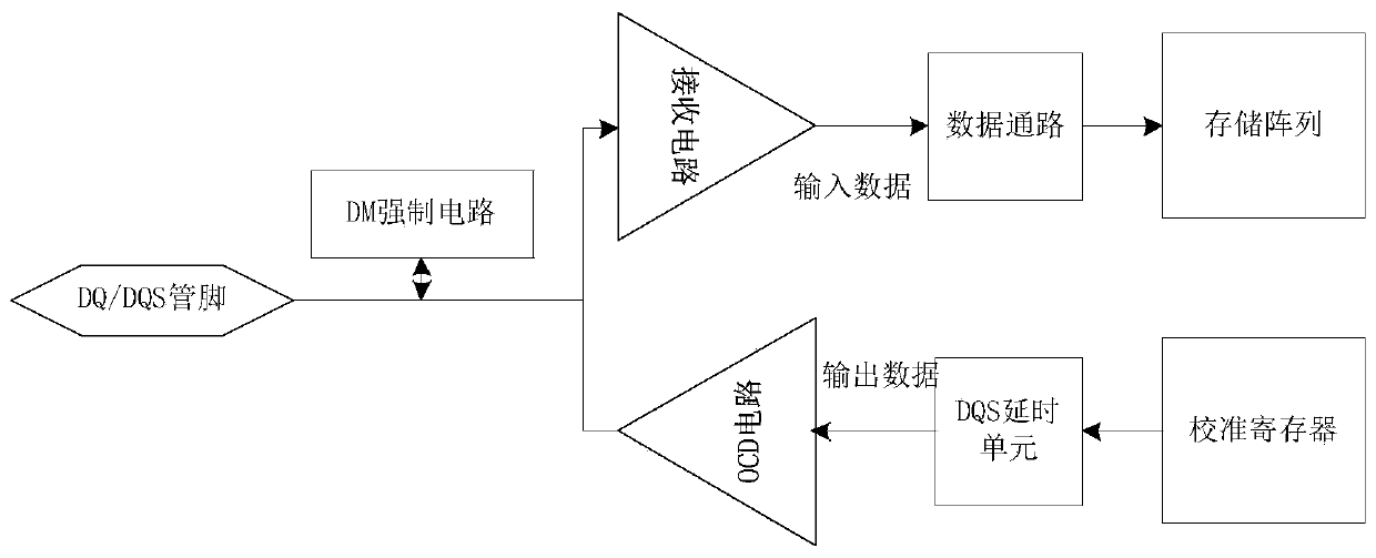
[0082] Specifically, such as image 3 As shown, the test process of DQ pins and DQS pins is as follows:

[0083] Step S11 power on the chip:

[0084] Specifically: enter the compression mode, and write the background data in the storage array;

[0085] Writing in compressed mode can save the number of pins that need to be connected in wafer testing, thereby greatly reducing the design and manufacturing cost of pin cards, increasing the number of simultaneous tests, and reducing the overall testing time.

[0086] Step S12 adjusts the compression mode to normal mode:

[0087] Specifically:

[0088] Use the DM forcing circuit to force the DM pin to be low, and the data is input and output normally; the purpose here is that the DM function of the DRAM does not work, and the data is read and written normally through the DQ / DQS pin.

[0089] Using the test mode, it is not necessary to connect the DM pins during wafer testing, which reduces the design and manufacturing costs of p...

Embodiment 2

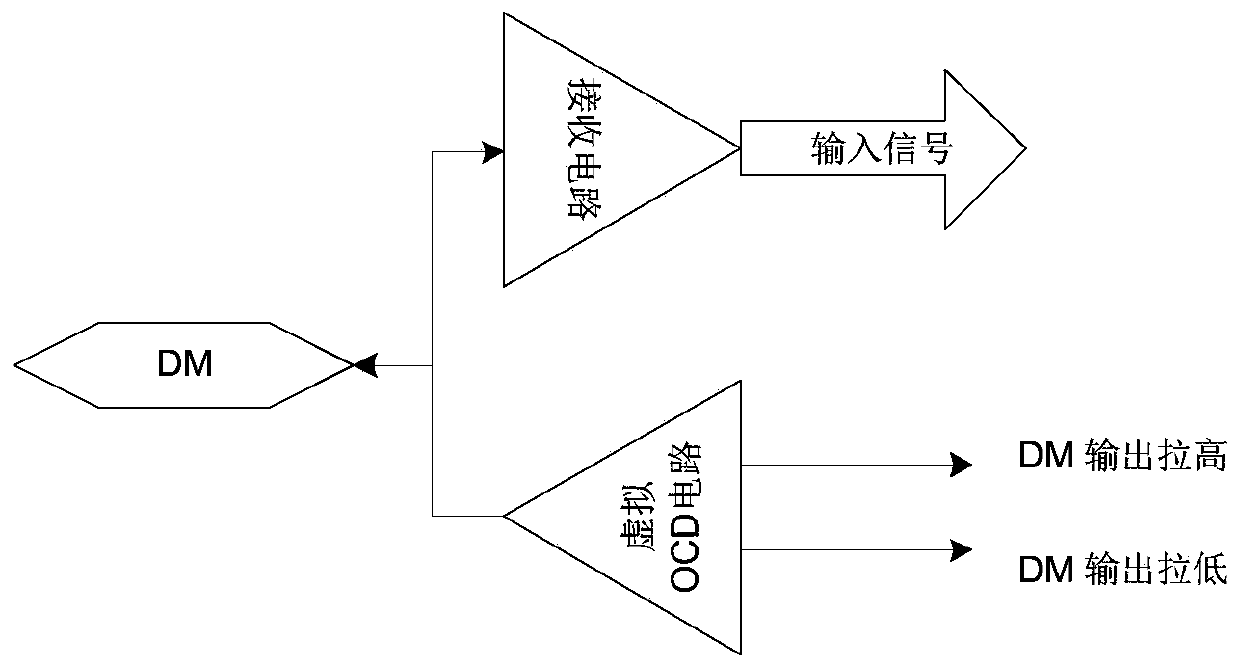
[0099] Take the DM pin as an example for illustration: specifically, as Figure 4 As shown, the test flow of the DM pin is as follows:

[0100] Step S21 power on the chip:

[0101] Specifically: enter the compression mode, write the background data in the storage array; write in the compression mode, save the number of pins that need to be connected in the wafer test, thereby greatly reducing the design and manufacturing cost of the needle card, and increasing the same test number, reducing the overall test time;

[0102] Step S22 adjusts the compressed mode to the normal mode:

[0103] Specifically: use the DM forcing circuit to force the DM pin to be high, and the data will be shielded. The purpose here is that the DM function of DRAM works, and the data passing through the DQ / DQS pin will be masked.

[0104] In this way, the DM pin does not need to be connected during the test, which reduces the design and manufacturing cost of the needle card, increases the number of s...

Embodiment 3

[0127] In the following embodiments, the DQ / DQS pin and the DM pin are judged respectively.

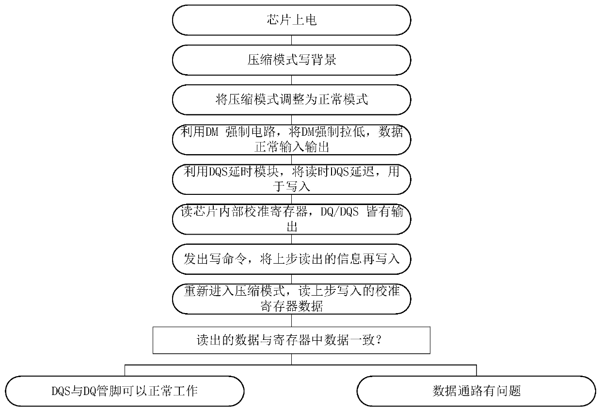
[0128] refer to Figure 6 , which describes in detail an example of testing the connection performance of all datapath pins in the wafer-level mass production test of a product.

[0129] Step S31: Storage array writes background data

[0130] The chip is powered on, enters the compression mode, and writes background data in the storage array; this background data needs to be different from the data in the specified calibration register to identify whether the data rewriting is successful;

[0131] This step can reuse the writing steps in the normal wafer test, which simplifies the test complexity; there is no need to increase the number of connections of DQ pins, DQS pins and DM pins;

[0132] Step S32: Resetting the read and write timing

[0133] Change the chip's RL (read latency, read latency, product configurable application parameters defined by JEDEC), BL (burst length, burst...


PUM


Abstract

The invention discloses a DRAM (dynamic random access memory) wafer-level pin connectivity test circuit and a method. The circuit structure comprises a calibration register, a delay unit, an OCD circuit, a receiving circuit, a data path and a storage array which are connected in sequence, input signals of a DQ pin and a DQS pin of a DRAM wafer level are transmitted into a chip through the receiving circuit, and output signals of the DQ pin and the DQS pin are driven through the OCD circuit. DM pin input signals of the DRAM wafer level are transmitted into the chip through the receiving circuit, and output signals of the DRAM wafer level control the level through the DM forced circuit. According to the invention, under the condition of not adding extra pin connection, the functions of all DQ data paths and DQS and DM pins are completely verified, the test comprehensiveness is improved, and the design difficulty and cost of the test pin card are not increased; for subsequent back-end testing, the bad chips are screened out in advance, the packaging cost is reduced, and the back-end testing yield is improved. And for KGD type products, the DPM is reduced, and the product quality is ensured.

Description

technical field [0001] The invention relates to the field of memory testing, in particular to a testing circuit and method for the connectivity of DRAM wafer-level pins. Background technique [0002] At present, the detection of the pin connectivity of DRAM chips (Dynamic Random Access Memory, that is, dynamic random access memory) is usually implemented at the granular level, because the packaging of the grains will lead out all the chip pins, and the testing machine can target each tube. Pin connectivity is tested. Also, due to the contradiction between the improvement of the number of chip measurements and the number of chip pin connections, the mass production test of DRAM wafers does not meet the conditions for realizing this test item. [0003] In the wafer test of DRAM, in order to increase the number of simultaneous tests of the chip and reduce the test cost, the chip usually works in a special test mode; in this mode, the data writing of the chip is realized by the...

Claims


Application Information

Patent Timeline
Patent Type & Authority Applications(China)
IPC IPC(8): G11C29/00G11C29/56
CPCG11C29/006G11C29/56
Inventor 王帆王可新汤子月刘凯
Owner XI AN UNIIC SEMICON CO LTD
Why Eureka
Try Eureka