Display panel and preparation method thereof, and display device
A technology for display panels and backplanes, which is used in the manufacture of semiconductor/solid-state devices, electrical components, and electrical solid-state devices. The effect of efficiency
- Summary
- Abstract
- Description
- Claims
- Application Information
AI Technical Summary
Problems solved by technology
Method used
Image

Examples
Embodiment 1
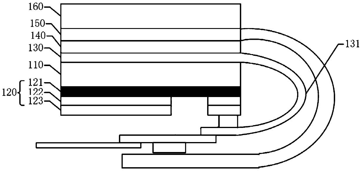
[0030] Such as figure 1 As shown, in this embodiment, the display panel 10 of the present invention includes a backplane layer 110 , a heat dissipation layer 120 , an OLED layer 130 , an optical glue 140 , a touch layer 150 and a polarizer layer 160 .
[0031] The backplane layer 110 is made of metal or other materials with good thermal conductivity and heat dissipation, and is attached and contacted with the heating components of the display panel through the heat conduction patch to achieve heat conduction. There are a plurality of radiating holes, so as to make use of the temperature difference effect between the inside and outside of the display panel 10 , so that the internal high-temperature gas and the external low-temperature gas can exchange heat in the form of heat convection through these radiating holes.
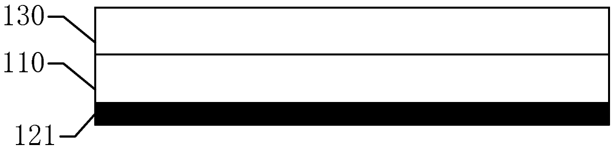
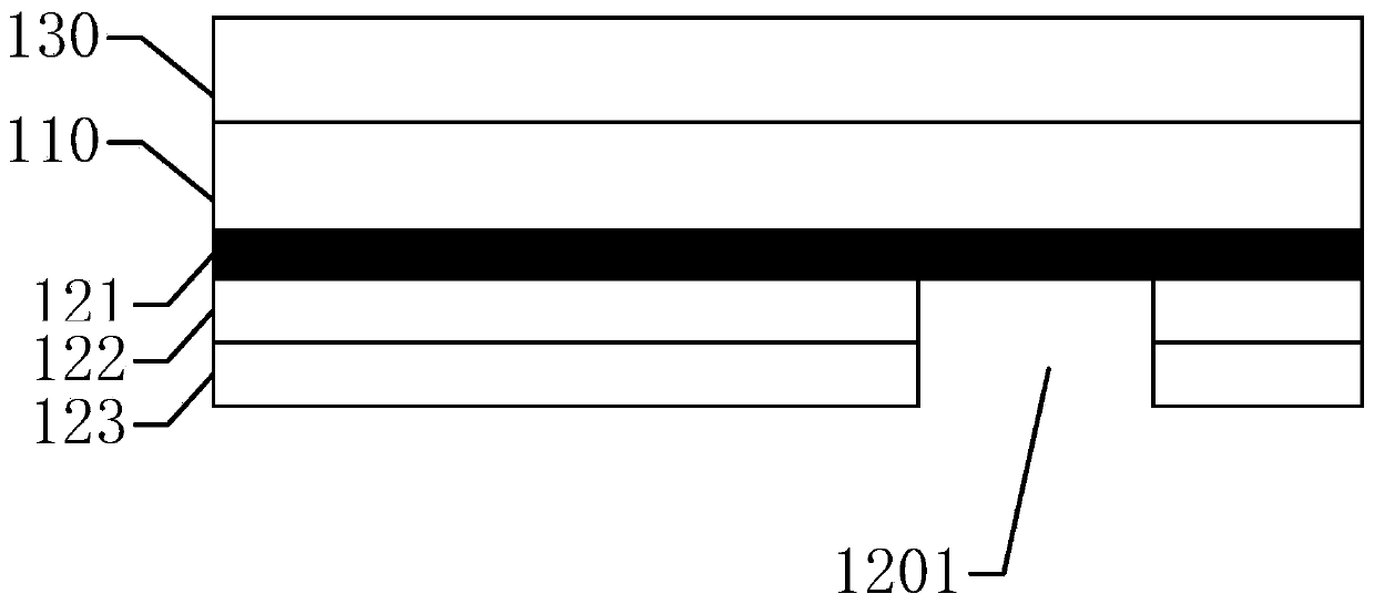
[0032] The heat dissipation layer 120 includes a graphite layer 121 , a foam layer 122 and a metal layer 123 .
[0033] Such as figure 2 As shown, the graphit...
PUM
| Property | Measurement | Unit |
|---|---|---|
| Width | aaaaa | aaaaa |
Abstract
Description
Claims
Application Information
 - Generate Ideas
- Intellectual Property
- Life Sciences
- Materials
- Tech Scout
- Unparalleled Data Quality
- Higher Quality Content
- 60% Fewer Hallucinations
Browse by: Latest US Patents, China's latest patents, Technical Efficacy Thesaurus, Application Domain, Technology Topic, Popular Technical Reports.
© 2025 PatSnap. All rights reserved.Legal|Privacy policy|Modern Slavery Act Transparency Statement|Sitemap|About US| Contact US: help@patsnap.com