Light homogenizing structure for optical lens

An optical lens, double-sided structure technology, applied in the field of optical components, can solve the problems of not being able to match the requirements of miniaturization well, not being able to effectively remove stripes, and the volume of the homogenizing device being large, etc., to achieve the best light field effect. , Keep the light field uniform transition, the effect of small volume

Pending Publication Date: 2020-02-28
宁波舜宇奥来技术有限公司
View PDF0 Cites 1 Cited by
  • Summary
  • Abstract
  • Description
  • Claims
  • Application Information

AI Technical Summary

Problems solved by technology

[0003] The light homogenizing device used in the existing TOF lens module is large in size and thick in thickness, which cannot well match the miniaturization needs of electronic devices such as mobile phones and tablet computers.
Moreover, the existing homogenization devices cannot effectively remove the fringe phenomenon, making the light field effect poor

Method used


Image

  • Light homogenizing structure for optical lens
  • Light homogenizing structure for optical lens
  • Light homogenizing structure for optical lens

Examples


Embodiment 1

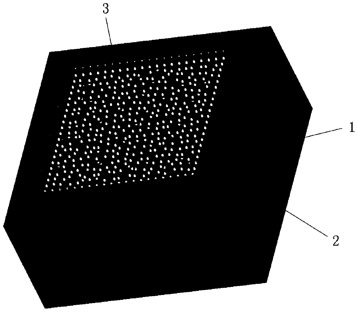
[0063] figure 1 It is a three-dimensional view of a single-sided single-layer convex microlens homogenizer; figure 2 It is the front view of the single-sided single-layer convex microlens homogenizer; image 3 It is a side view of a single-sided single-layer convex microlens homogenizer; Figure 4 An example diagram of the two-dimensional distribution of the center point and shape aperture of the single-sided single-layer convex microlens feature; Figure 5 An example graph of the 2D distribution of microlens features generated for a single-sided single-layer convex 2D center point and shape arrangement; Image 6 It is an example diagram of the three-dimensional structure of the single-sided single-layer convex microlens characteristic; Figure 7 An example diagram of the far-field outgoing light field distribution for random microlenses arranged with a dodging sheet.

[0064] combine Figure 1-Figure 7 In this embodiment, the uniform light structure is a single-sided si...

Embodiment 2

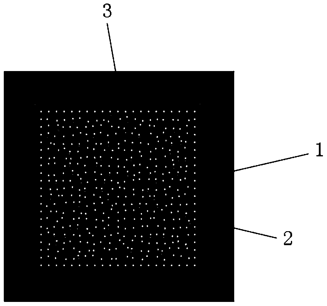
[0069] Figure 8 An example diagram of the two-dimensional distribution of the center point and shape aperture of a single-sided single-layer convex microlens; Figure 9 An example graph of the two-dimensional distribution of microlens features generated for the two-dimensional center point and shape arrangement of a single-sided single-layer convex microlens; Figure 10 It is an example diagram of the three-dimensional distribution of the single-sided single-layer convex microlens structure; Figure 11 It is an example diagram of the cross-section of the characteristic part of the single-sided single-layer convex microlens structure; Figure 12 It is an enlarged example diagram of the voronoi boundary of a part of a single-sided single-layer convex microlens area; Figure 13 An enlarged example of a single-sided single-layer convex microlens structure; Figure 14 An example diagram of the far-field exit angle distribution of the random microlens arrangement homogenizer pro...

Embodiment 3

[0075] Figure 16 It is an example diagram of the three-dimensional distribution of the single-sided single-layer concave microlens structure; Figure 17 It is an example diagram of the cross-section of the characteristic part of the single-sided single-layer concave microlens structure; Figure 18 It is a schematic diagram of the cross-section of the single-sided single-layer concave microlens structure area plus the matrix.

[0076] combine Figure 16-Figure 18 In this embodiment, the uniform light structure is a single-sided single-layer convex microlens structure, including: a substrate, a UV glue layer, a microlens layer, an air layer, a VCSEL light source chip, and a chip fixing substrate on which the light source chip is mounted. In this embodiment, the shape of the microlens is the straight boundary polygon formed by the voronoi boundary, and the center of the microlens is the definition point of the Voronoi boundary. , completely random. The distance between any t...


PUM

PropertyMeasurementUnit
thicknessaaaaaaaaaa
thicknessaaaaaaaaaa
thicknessaaaaaaaaaa

Abstract

The invention relates to a light homogenizing structure for a single optical lens. The structure comprises a substrate, a light source chip, an adhesive layer and a microlens layer, wherein the adhesive layer is arranged on one surface of the substrate; the microlens layer is arranged on the adhesive layer; an air layer is arranged between the microlens layer and the light source chip; the microlens layer is formed by randomly distributing a plurality of microlenses on the adhesive layer. According to the light homogenizing structure for the optical lens, the thickness of a TOF module can be controlled within 2mm as a whole, so that the light homogenizing structure can be applied to miniaturized equipment; the structure can well remove the striation phenomenon of periodic and micro-periodic microlens arrays, and maintain uniform transition of light fields; the overall filling coefficient of the surface type can reach 99%, so that the maximum utilization rate of incident light beams isensured, and the best light field effect is achieved; and the joint has no cross section, so that the processing difficulty of the mother board gray scale mask and product nano-imprinting is reduced,the possibility of residual glue on the template is reduced, and the overall processing precision and efficiency are improved.

Description

technical field [0001] The invention relates to the field of optical elements, in particular to a light homogenization mechanism for an optical lens, in particular to a light homogenization structure for a TOF lens module. Background technique [0002] TOF lens modules are widely used in the fields of face recognition and three-dimensional detection technology. With the development trend of miniaturization of electronic equipment such as mobile phones and tablet computers, TOF lens modules are also gradually becoming smaller. As an important The components of uniform light devices must also meet the current development needs with a thinner and thinner posture. [0003] The light homogenizing device used in the existing TOF lens module is large in size and thick in thickness, which cannot well meet the miniaturization requirements of electronic devices such as mobile phones and tablet computers. Moreover, the existing uniform light device cannot effectively remove the fringe...

Claims


Application Information

Patent Timeline
Patent Type & Authority Applications(China)
IPC IPC(8): G02B27/09G02B3/00
CPCG02B3/0037G02B3/0043G02B27/0927G02B27/0961
Inventor 吴沣原
Owner 宁波舜宇奥来技术有限公司
Why Eureka
Try Eureka