Manufacturing process of low electromagnetic interference power device terminal structure

A technology that interferes with power and manufacturing process. It is used in semiconductor/solid-state device manufacturing, electrical solid-state devices, and electrical components. It can solve the problem of increasing device process steps, reducing high-frequency and high-amplitude electromagnetic interference, and increasing device switching losses. problem, to achieve the effect of alleviating EMI noise

A technology that interferes with power and manufacturing process. It is used in semiconductor/solid-state device manufacturing, electrical solid-state devices, and electrical components. It can solve the problem of increasing device process steps, reducing high-frequency and high-amplitude electromagnetic interference, and increasing device switching losses. problem, to achieve the effect of alleviating EMI noise

CN110854072AActive Publication Date: 2020-02-28四川民承电子有限公司

Image

  • Manufacturing process of low electromagnetic interference power device terminal structure
  • Manufacturing process of low electromagnetic interference power device terminal structure
  • Manufacturing process of low electromagnetic interference power device terminal structure

Examples


Embodiment Construction

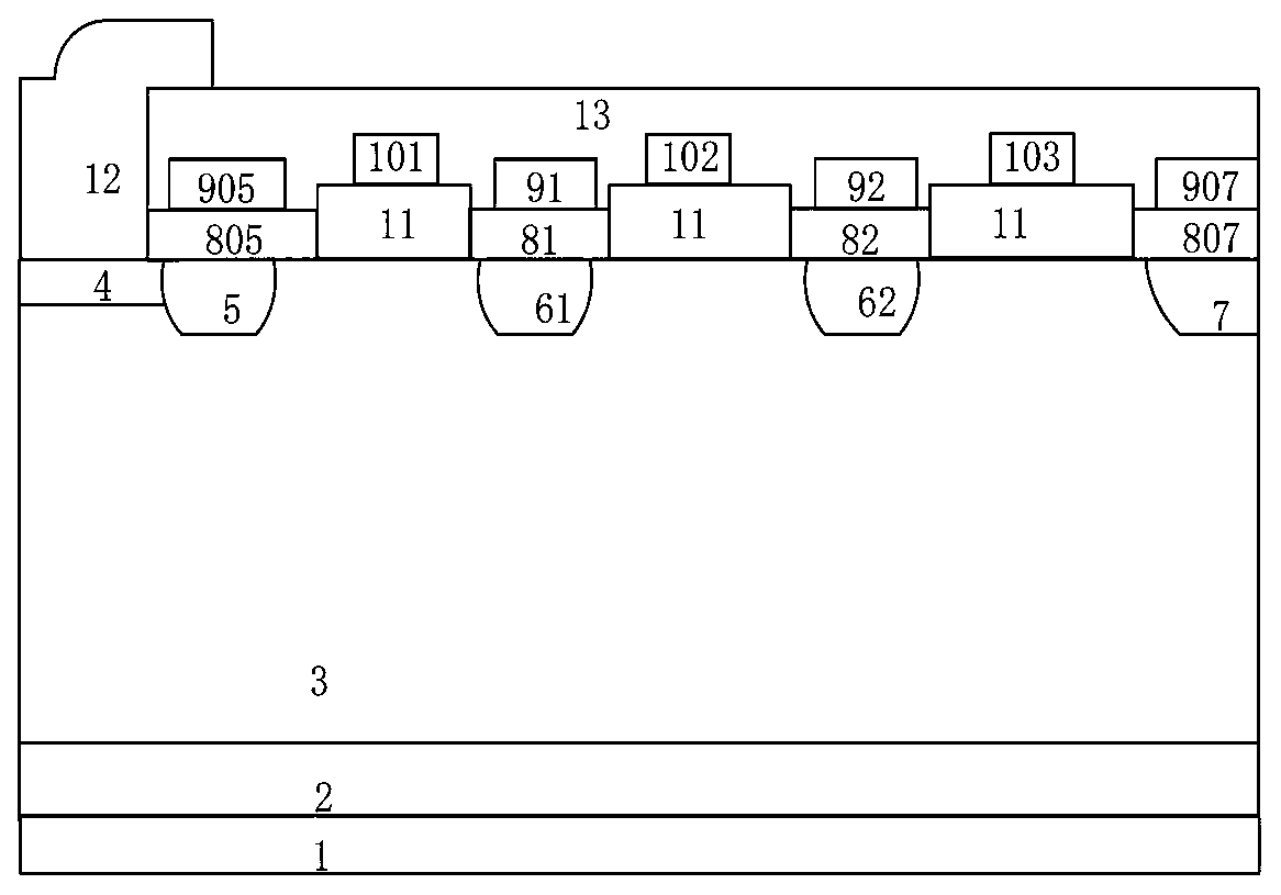
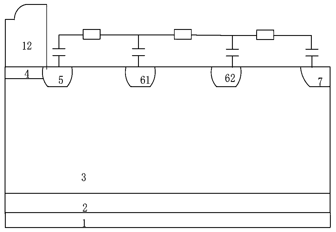
[0014] Hereinafter, the terminal structure of the low electromagnetic interference power device of the present invention will be described in detail with reference to exemplary embodiments.

[0015] figure 1 A schematic flow chart of an exemplary embodiment of the manufacturing process of the low electromagnetic interference power device terminal structure of the present invention is shown.

[0016] Such as figure 1 As shown, in an exemplary embodiment of the present invention, the manufacturing process of the low electromagnetic interference power device terminal structure includes the following steps:

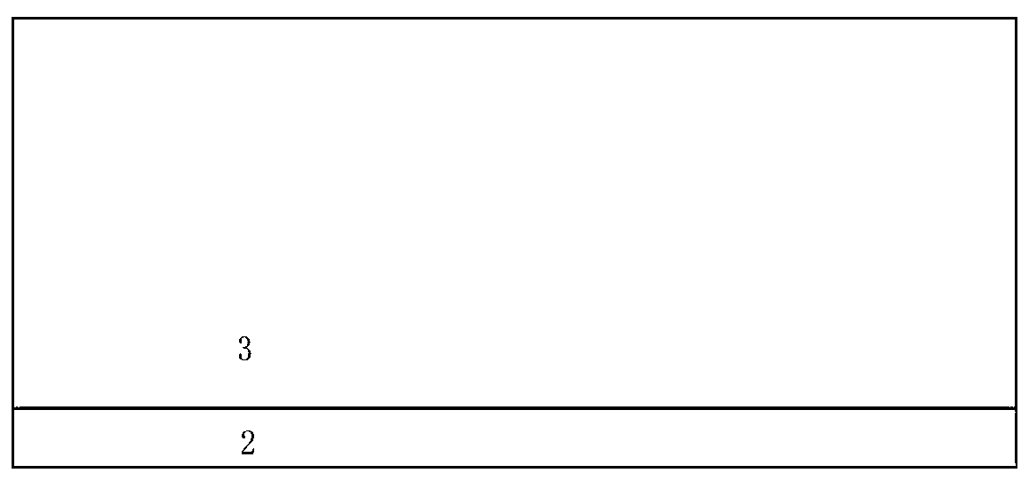
[0017] S01, growing a first conductivity type semiconductor epitaxial layer on a first conductivity type semiconductor substrate. The first conductivity type semiconductor epitaxial layer may have a predetermined withstand voltage requirement and a predetermined thickness, for example, the predetermined withstand voltage requirement may be 600V or higher; the predetermined ...


PUM


Abstract

The invention provides a manufacturing process of a low electromagnetic interference power device terminal structure. The terminal structure manufactured by the process comprises a metallized drain electrode, a first conductive type semiconductor substrate and a first conductive type semiconductor epitaxial layer, a second conductive type semiconductor main junction, a second conductive type semiconductor equipotential ring, a first conductive type cut-off ring, a second conductive type semiconductor field limiting ring, a first dielectric layer, a second dielectric layer, a third dielectric layer, a conductive field plate, a resistor and a metallized source electrode which are stacked from bottom to top. In the invention, an HK dielectric layer can be introduced between the field limitingring and the field plate. An MIS capacitor structure is formed by the semiconductor field limiting ring, the HK dielectric layer and the field plate and is connected in series with an adjacent polycrystalline silicon resistor so that an RC absorption network is formed between high potentials of the source electrode and the drain electrode, dv / dt and di / dt generated by a power device in a fast switch can be effectively inhibited, and an EMI noise is relieved.

Description

technical field [0001] The invention relates to the field of power semiconductor devices, in particular to a manufacturing process of a power device terminal structure. Background technique [0002] Usually, the typical application environment of power devices is switching power supply. In order to meet the miniaturization requirements of switching power supply, its switching frequency and power density are constantly increasing. Modularization and functional integration can improve the power density of electronic components, but it will also produce more and more The increasingly complex internal electromagnetic environment. When the power device is in the fast switching state, its voltage and current change sharply in a short time, resulting in high dv / dt and di / dt, which become a strong source of electromagnetic interference. [0003] In terms of electromagnetic interference (EMI) suppression technology, one is to reduce high-frequency and high-amplitude electromagnetic ...

Claims


Application Information

Patent Timeline
28 Feb 2020
Publication
CN110854072A
IPC
H01L21/82; H01L23/552; H01L27/02
CPC
H01L21/82; H01L27/0288; H01L23/552
Inventors
蔡少峰; 任敏