P-type silicon carbide ohmic contact structure and manufacturing method thereof

A technology of ohmic contact and silicon carbide, which is applied in the direction of electrical components, circuits, semiconductor devices, etc., can solve the problems of rising device on-state resistance and affecting device performance, so as to improve device reliability, maintain consistent thermal expansion coefficient, and save process costs Effect

Pending Publication Date: 2020-02-28
HANGZHOU DIANZI UNIV
View PDF3 Cites 0 Cited by
  • Summary
  • Abstract
  • Description
  • Claims
  • Application Information

AI Technical Summary

Problems solved by technology

If the reliability of the ohmic contact resistance is poor, the on-state resistance of the device will increase, which will affect the performance of the device in serious cases

Method used


Image

  • P-type silicon carbide ohmic contact structure and manufacturing method thereof
  • P-type silicon carbide ohmic contact structure and manufacturing method thereof
  • P-type silicon carbide ohmic contact structure and manufacturing method thereof

Examples


Embodiment Construction

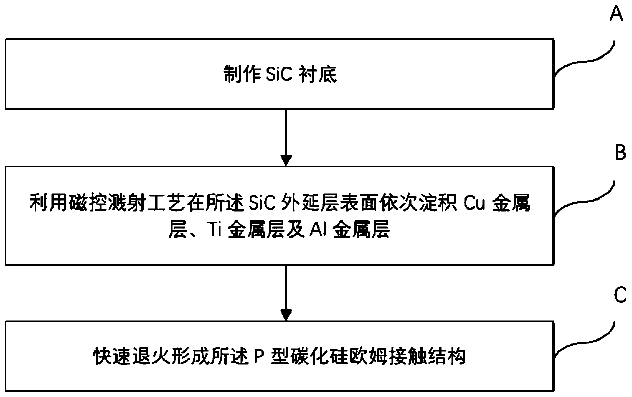
[0033] The following will clearly and completely describe the technical solutions in the embodiments of the present invention with reference to the accompanying drawings in the embodiments of the present invention. Obviously, the described embodiments are only some, not all, embodiments of the present invention. Based on the embodiments of the present invention, all other embodiments obtained by persons of ordinary skill in the art without creative efforts fall within the protection scope of the present invention.

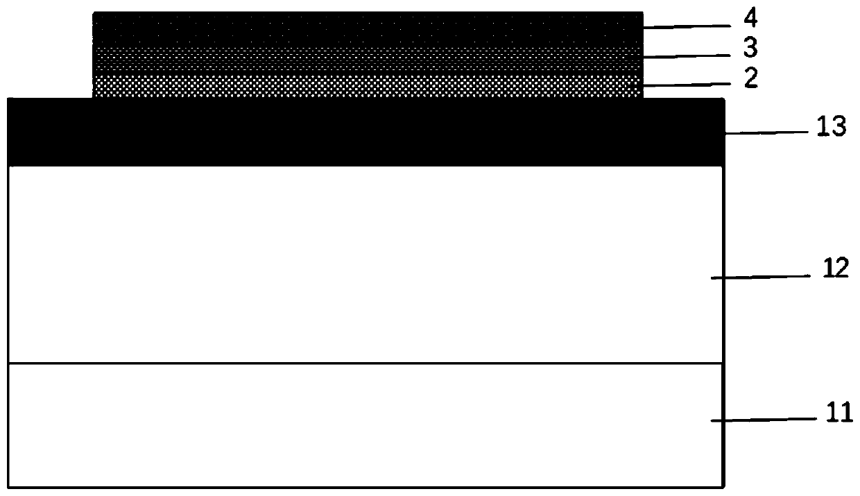
[0034] figure 1 A cross-sectional view of the structure of a P-type silicon carbide ohmic contact provided for the embodiment of the present invention, as shown in the figure:

[0035] SiC substrate 11 is provided with SiC N - Epitaxial layer 12; SiC N - The epitaxial layer 12 is provided with silicon carbide P + Epitaxial layer 13;

[0036] SiC P + The epitaxial layer 13 is provided with a Cu metal layer 2, the Cu metal layer 2 is provided with a Ti metal lay...


PUM

PropertyMeasurementUnit
thicknessaaaaaaaaaa
thicknessaaaaaaaaaa
thicknessaaaaaaaaaa

Abstract

The invention relates to a P-type silicon carbide ohmic contact structure and a manufacturing method thereof. The manufacturing method comprises the following steps: selecting a SiC epitaxial substrate, sequentially depositing a Cu metal layer, a Ti metal layer and an Al metal layer on the surface of the substrate by a magnetron sputtering process, and rapidly annealing to form the P-type siliconcarbide ohmic contact structure. According to the invention, Cu metal material is used in the P-type silicon carbide ohmic contact structure, and can be combined with the power element crimping packaging technology of sintered copper. Both ohmic contact and packaging adopt Cu metal having the same thermal expansion coefficient and more applicability, thus being conducive to improve the reliabilityof the device and save the process cost.

Description

technical field [0001] The invention belongs to the field of manufacturing silicon carbide devices, in particular to a P-type SiC / Cu / Ti / Al ohmic contact structure and a manufacturing method. Background technique [0002] Compared with traditional germanium and silicon materials, the advantages of the third-generation wide-bandgap semiconductor silicon carbide mainly include: the electric field withstand capacity is about ten times that of silicon materials, the band gap is about three times that of silicon materials, and the thermal conductivity is about 10 times that of silicon materials. Triple and so on. The above material characteristics make it show the incomparable advantages of traditional silicon-based devices under the conditions of extreme temperature (especially high temperature), high voltage, high frequency and high power, and strong radiation. [0003] Ohmic contact is a key process technology in semiconductor manufacturing. Its purpose is to make the pressure...

Claims


Application Information

Patent Timeline
Patent Type & Authority Applications(China)
IPC IPC(8): H01L29/45H01L29/16
CPCH01L29/45H01L29/1608
Inventor 王颖隋金池曹菲包梦恬
Owner HANGZHOU DIANZI UNIV
Why Eureka
Try Eureka