

Preparation method for polycrystalline silicon function layer
A polysilicon layer and functional layer technology, which is applied in the manufacture of semiconductor/solid-state devices, electrical components, circuits, etc., can solve the problems of a large number of charges, the device is prone to leakage, and the thickness uniformity is not easy to control, etc., to improve high-frequency performance. , the effect of reducing the number of internal charges, excellent deposition uniformity
- Summary
- Abstract
- Description
- Claims
- Application Information
AI Technical Summary
Problems solved by technology
Method used
Image


Examples
preparation example Construction
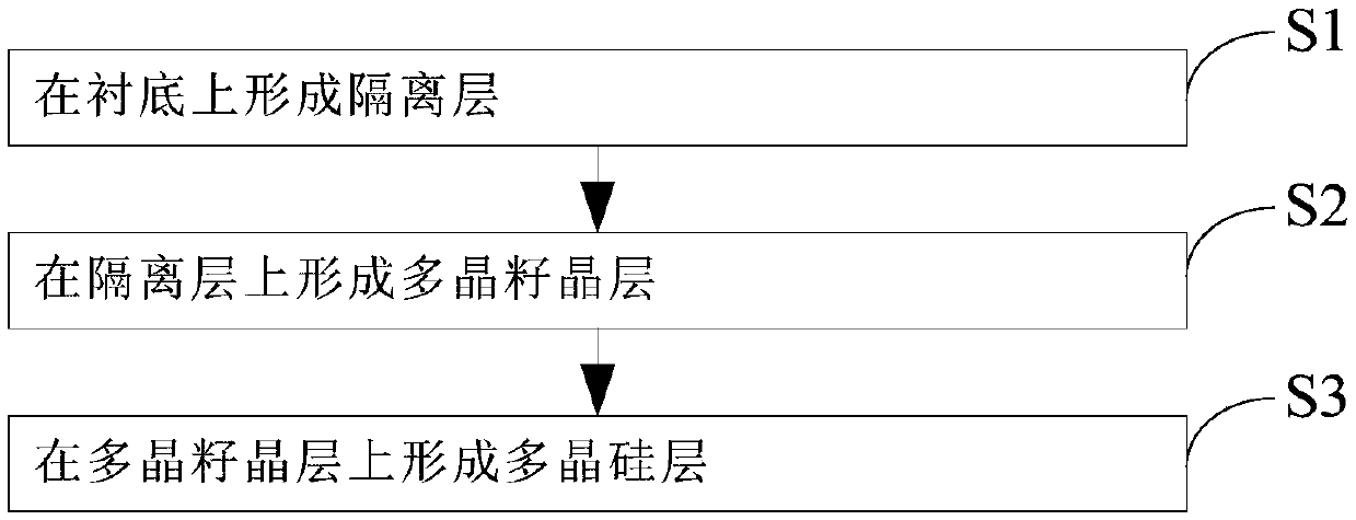
[0033] Please also refer to figure 1 and figure 2 , the preparation method of polysilicon functional layer provided by the invention, it comprises:
[0034] S1, forming an isolation layer on the substrate;
[0035] S2, forming a polycrystalline seed layer on the isolation layer;
[0036] S3, forming a polysilicon layer on the polycrystalline seed layer.
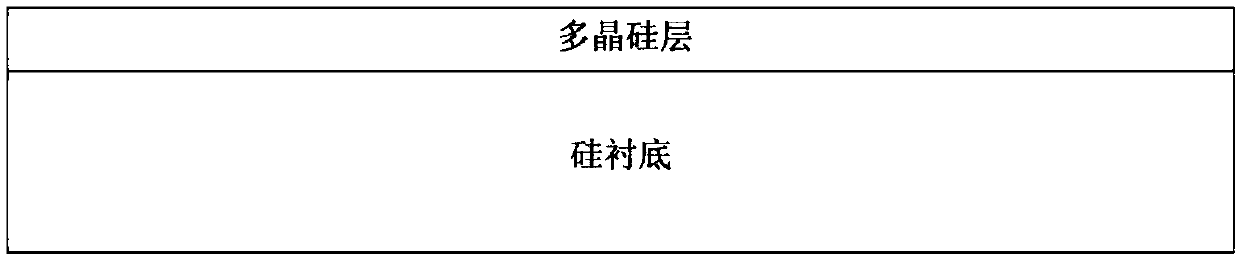
[0037] The substrate is a silicon substrate. Optionally, the isolation layer is a silicon dioxide layer.
[0038] With the help of the isolation layer, the interface state of the polysilicon layer can be guaranteed, and the formation of a low-resistance layer can be avoided, thereby improving the high-frequency performance of the material.
[0039] With the help of the polycrystalline seed layer, due to its highly controllable deposition parameters and excellent deposition uniformity, it can reduce the number of charges inside the polycrystalline silicon functional layer and improve the controllability of the thickness ...
PUM
| Property | Measurement | Unit |
|---|---|---|
| thickness | aaaaa | aaaaa |
| thickness | aaaaa | aaaaa |
Abstract
Description
Claims
Application Information