Semiconductor structure and forming method thereof

A semiconductor and gas flow technology, applied in semiconductor devices, semiconductor/solid-state device manufacturing, electrical components, etc., can solve problems such as increased leakage current, weakened channel current control ability, short channel effect, etc. Density, improve electrical performance, reduce loss effect

Active Publication Date: 2020-03-20
SEMICON MFG INT (SHANGHAI) CORP +1
View PDF4 Cites 0 Cited by
  • Summary
  • Abstract
  • Description
  • Claims
  • Application Information

AI Technical Summary

Problems solved by technology

Therefore, with the increase in the density and integration of semiconductor devices, the gate size of planar transistors is getting shorter and shorter. The control ability of traditional planar transistors on channel current becomes weaker, and the short channel effect occurs, which causes the leakage current to increase. Affect the electrical performance of semiconductor devices

Method used


Image

  • Semiconductor structure and forming method thereof
  • Semiconductor structure and forming method thereof
  • Semiconductor structure and forming method thereof

Examples


Embodiment Construction

[0026] Semiconductor devices still suffer from poor performance. The reasons for the poor performance of the device are analyzed in conjunction with a method of forming a semiconductor structure.

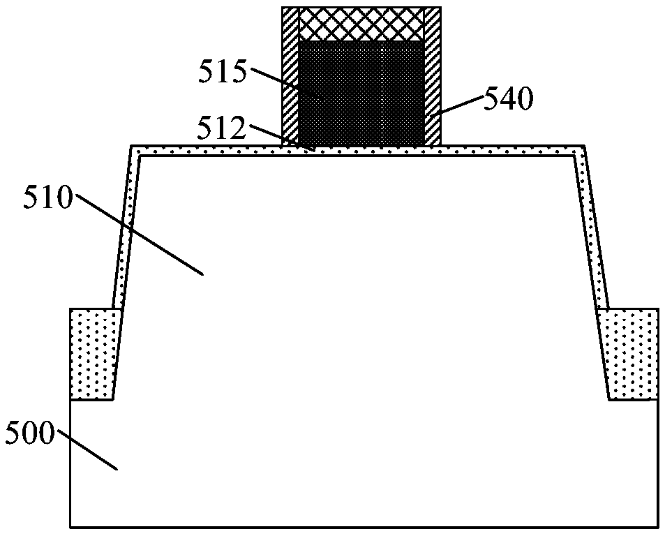
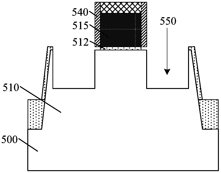
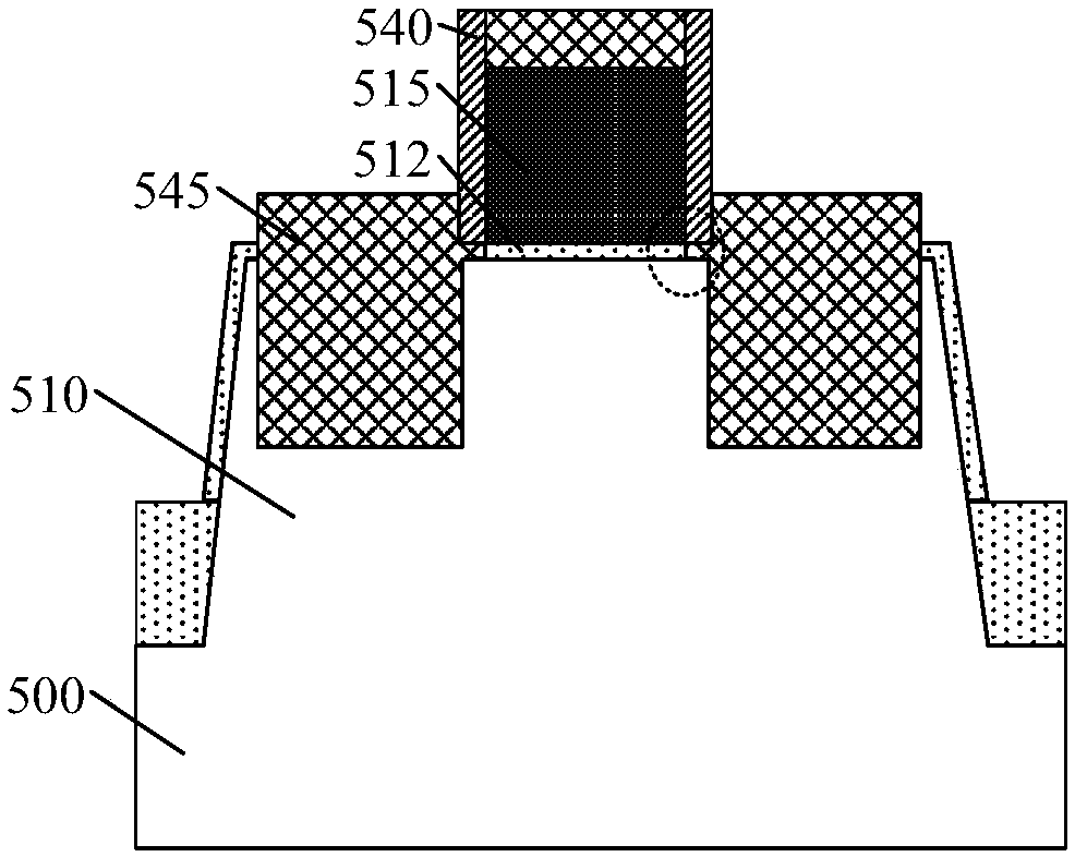
[0027] refer to Figure 1 to Figure 3 , shows a structural schematic diagram corresponding to each step in a method for forming a semiconductor structure.

[0028] refer to figure 1 , forming a base, the base includes a substrate 500, a fin 510 protruding from the substrate 500; forming a gate dielectric layer 512 on the surface of the fin 510; forming a gate layer across the fin 510 515, the gate layer 515 covers part of the top and part of the sidewall of the gate dielectric layer 512; a sidewall 540 is formed on the sidewall of the gate layer 515, and the sidewall 540 covers the gate layer Part of the gate dielectric layer 512 on both sides of 515.

[0029] refer to figure 2 , using the sidewall 540 as a mask, etching the fins 510 on both sides of the gate layer 515 to form...


PUM


Abstract

The invention discloses a semiconductor structure and a forming method thereof. The forming method comprises the steps that a base is formed, the base comprises a substrate, a fin part protruding outof the substrate, a gate dielectric layer covering the surface of the fin part and a gate electrode layer stretching across the fin part, the gate electrode layer covers part of the top and part of the side wall of the gate dielectric layer, and nitrogen ions are doped in the gate dielectric layer exposed out of the gate electrode layer; forming a side wall on the side wall of the gate layer; etching the fin parts on the two sides of the gate layer by taking the side walls as masks, and forming grooves in the fin parts on the two sides of the gate layer; and forming a source-drain doped layerin the groove. According to the embodiment of the invention, the probability of loss of the gate dielectric layer at the bottom of the side wall can be reduced, thereby facilitating the reduction of the probability of short circuit between the source-drain doped layer in the groove and the gate layer, and further facilitating the improvement of the electrical performance of the semiconductor structure.

Description

technical field [0001] The invention relates to the field of semiconductor manufacturing, in particular to a semiconductor structure and a forming method thereof. Background technique [0002] With the rapid development of semiconductor manufacturing technology, semiconductor devices are developing towards higher component density and higher integration. Transistors are currently being widely used as one of the basic semiconductor devices. Therefore, with the increase in the density and integration of semiconductor devices, the gate size of planar transistors is getting shorter and shorter. The control ability of traditional planar transistors on the channel current becomes weaker, and the short channel effect occurs, causing the leakage current to increase. affect the electrical performance of semiconductor devices. [0003] In order to better adapt to the reduction of feature size, the semiconductor process has gradually begun to transition from planar MOSFETs to three-d...

Claims


Application Information

Patent Timeline
Patent Type & Authority Applications(China)
IPC IPC(8): H01L21/336H01L29/78H01L21/306
CPCH01L29/785H01L29/66795H01L21/30604
Inventor 周飞
Owner SEMICON MFG INT (SHANGHAI) CORP
Why Eureka
Try Eureka