Image sensor with novel layout

An image sensor and layout technology, applied in the field of image sensors, can solve the problems of reduced pixel circuit sensitivity, increased floating diffusion point FD point capacitance, etc., to achieve the effect of improving quantum efficiency, high aperture ratio, and small capacitance

Pending Publication Date: 2020-03-20
思特威(上海)电子科技股份有限公司
View PDF1 Cites 0 Cited by
  • Summary
  • Abstract
  • Description
  • Claims
  • Application Information

AI Technical Summary

Problems solved by technology

Application Publication No. CN102184931A, the patent titled "Image Sensor" discloses the arrangement of image sensor pixel units. In various arrangement schemes, the arrangement of the reset transistor and the source follower transistor will make the floating diffusion point FD point Capacitance increases, pixel circuit sensitivity decreases

Method used


Image

  • Image sensor with novel layout
  • Image sensor with novel layout
  • Image sensor with novel layout

Examples


Embodiment Construction

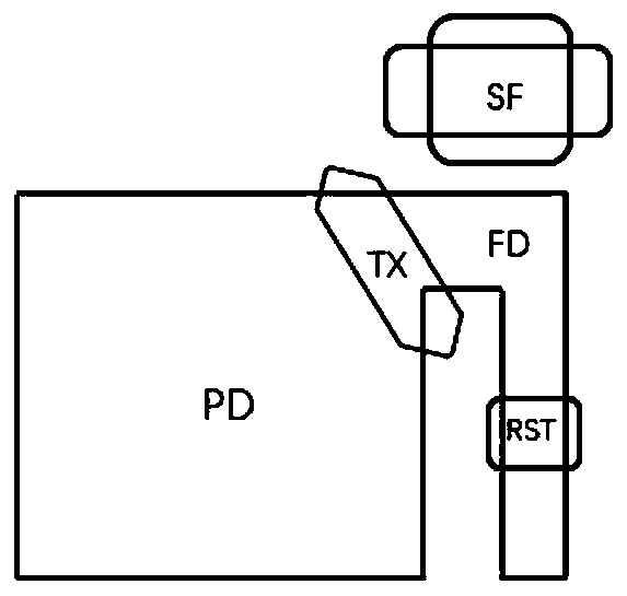
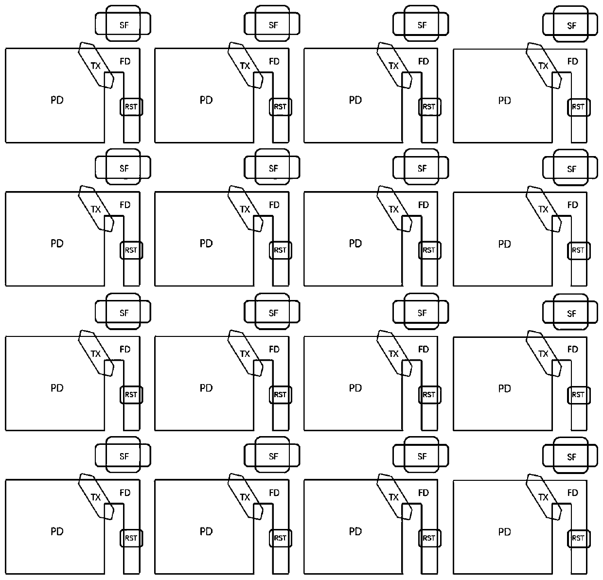
[0026] The scheme proposed by the patent of the present invention will be described in detail below in conjunction with each accompanying drawing. Each device and its identification in each drawing of the present invention is for the purpose of illustrating device arrangement or layout structure, and does not limit the specific shape, size or specific angle of each currently marked device. In the specific circuit design, it can be designed as a corresponding shape according to the specific application.

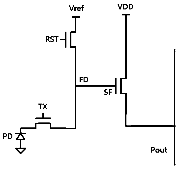
[0027] figure 1 It is a pixel circuit diagram of an embodiment of an image sensor with a new structural layout provided by the present invention, as shown in the figure, it is a 3-transistor image sensor structure. The photodiode PD and the transfer transistor TX form a photosensitive unit, which converts photons into electrons and transfers them to the floating diffusion FD. The reset crystal RST is connected between the variable voltage source Vref and the floating diffusi...


PUM


Abstract

The invention provides an image sensor with a novel layout structure. The image sensor comprises a pixel array composed of a plurality of pixel units arranged in rows and columns, each pixel unit comprises a photosensitive unit, and each photosensitive unit comprises a photodiode and a transmission transistor; the transmission transistor is arranged at the corner of the photodiode along an inclination angle; wherein the arrangement structure of the transmission transistor forms an opening, and the floating diffusion point is arranged at the opening; and the source following transistor is arranged at the corner position of the pixel unit and is close to the floating diffusion point. The pixel unit can further comprise a conversion gain control transistor which is arranged on the same side of the reset transistor. According to the novel structure layout image sensor provided by the invention, the floating diffusion point capacitance of the pixel unit is small, the pixel circuit conversion gain is high, and the performance of the image sensor can be effectively improved.

Description

technical field [0001] The present invention relates to image sensor technology, in particular to an image sensor with a novel design layout. Background technique [0002] CMOS image sensors are widely used in various fields, such as smartphones, surveillance equipment, drones, and artificial intelligence, and their design requirements are increasingly miniaturized. With the development of technology, the size of the image sensor pixel unit is further reduced, increasing the conversion gain of the pixel circuit and improving the sensitivity of the image sensor is the direction of its development and improvement. [0003] In the design of the image sensor, adopting a reasonable structural layout can effectively improve the performance of the image sensor. For example, the layout configuration is compact, and the components in the pixel unit are arranged reasonably, which can increase the quantum efficiency of the photosensitive unit. A common image sensor adopts a 4T struct...

Claims


Application Information

Patent Timeline
Patent Type & Authority Applications(China)
IPC IPC(8): H01L27/146
CPCH01L27/14605H01L27/14612H01L27/14643H01L27/14609H04N25/767H04N25/766H04N25/75
Inventor 徐辰王欣莫要武邵泽旭石文杰
Owner 思特威(上海)电子科技股份有限公司
Why Eureka
Try Eureka