

Wafer position identification system and method
An identification system and identification method technology, which is applied in the field of wafer position identification system, can solve problems such as wafer scratches, laminations or skewed wafers, and achieve the effect of preventing wafer scratches and improving yield
- Summary
- Abstract
- Description
- Claims
- Application Information
AI Technical Summary
Problems solved by technology
Method used
Image

Examples
Embodiment Construction
[0034] The specific implementation manner of the present invention will be described in more detail below with reference to schematic diagrams. The advantages and features of the present invention will be more apparent from the following description. It should be noted that all the drawings are in a very simplified form and use imprecise scales, and are only used to facilitate and clearly assist the purpose of illustrating the embodiments of the present invention.
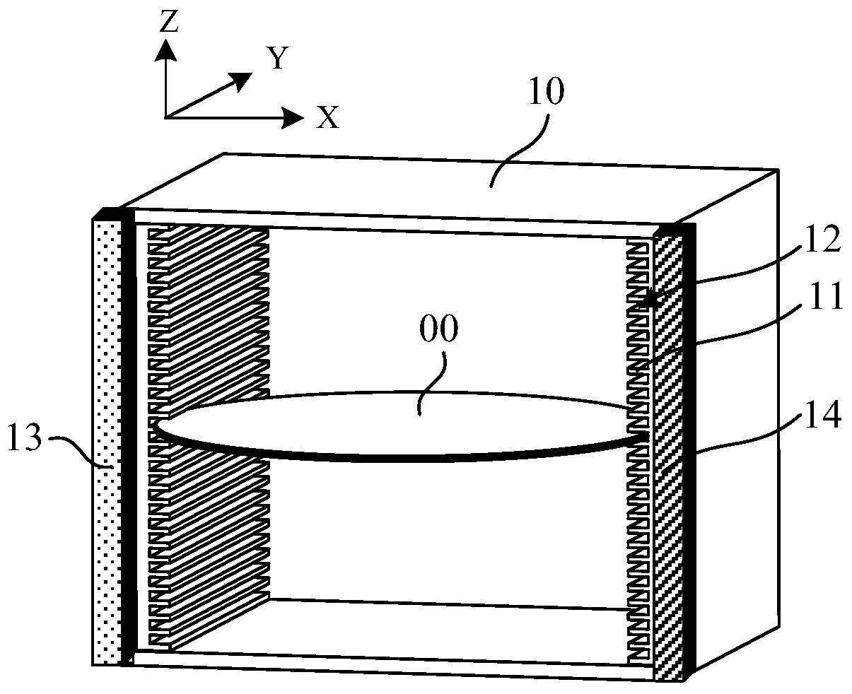
[0035] figure 1 A schematic structural diagram of the wafer position identification system provided in this embodiment. Such as figure 1 As shown, the present embodiment provides a wafer position recognition system, including:
[0036] The wafer carrier module 10 includes a plurality of storage positions 12 overlapping in the vertical direction, and has an opening;
[0037] A light source module 13, arranged on one side of the opening, for emitting parallel detection light along the horizontal direction;
[00...
PUM
 Abstract
Description
Claims
Application Information