Film bulk acoustic resonator and manufacturing method thereof

A thin-film bulk acoustic wave and manufacturing method technology, applied in the direction of electrical components, impedance networks, etc., can solve the problems of film thickness distortion of the piezoelectric layer and its electrodes, influence of device structure reliability, complex and cumbersome process, etc., to improve crystal quality , low cost and simple process

Pending Publication Date: 2020-04-03
SUZHOU INST OF NANO TECH & NANO BIONICS CHINESE ACEDEMY OF SCI
View PDF4 Cites 4 Cited by
  • Summary
  • Abstract
  • Description
  • Claims
  • Application Information

AI Technical Summary

Problems solved by technology

Around November 2017, the Ministry of Industry and Information Technology of China officially delineated the range of the mid-frequency band of the 5G system, and no longer accepted and approved other adjacent frequency bands for new applications. The advancement of the 5G era has brought new challenges to the resonator, produced by Fujitsu, Japan The structure of the FBAR and its related products is relatively diverse. Judging from the relevant patents applied by the company, the structure of its FBAR can be roughly divided into two categories: air cavity type (such as patent US7323953B2) and air gap (such as patent US20100060384A1), in which the air The gap needs to be filled with a sacrificial layer, and then ground and polished, the process is complex and cumbersome
For the traditional thin-film bulk acoustic resonator using metal as the electrode, the loss is large. At the same time, because the piezoelectric film is deposited or sputtered on the patterned electrode, there is stress at the step, which will cause the piezoelectric layer and its electrode. The thickness is distorted here, causing stress concentration and affecting the reliability of the device structure.
As well as traditional devices, steps will be generated after the lower electrode is patterned, and there will be stress at the steps, which will cause the film thickness of the piezoelectric layer and its electrodes to be distorted here, resulting in stress concentration, which will affect the reliability of the device structure.

Method used


Image

  • Film bulk acoustic resonator and manufacturing method thereof
  • Film bulk acoustic resonator and manufacturing method thereof
  • Film bulk acoustic resonator and manufacturing method thereof

Examples


Embodiment 1

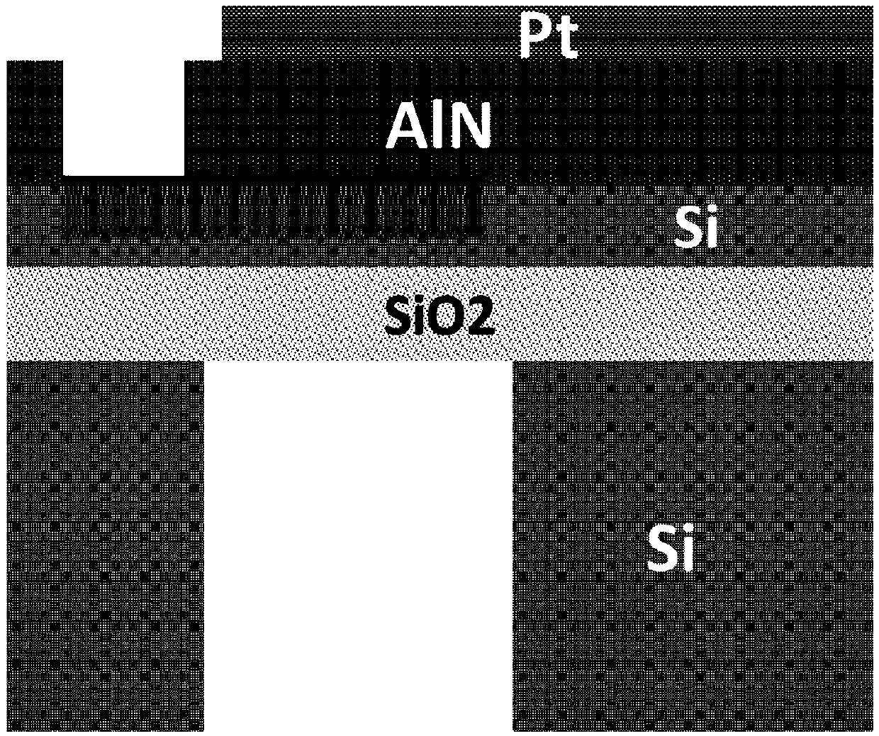
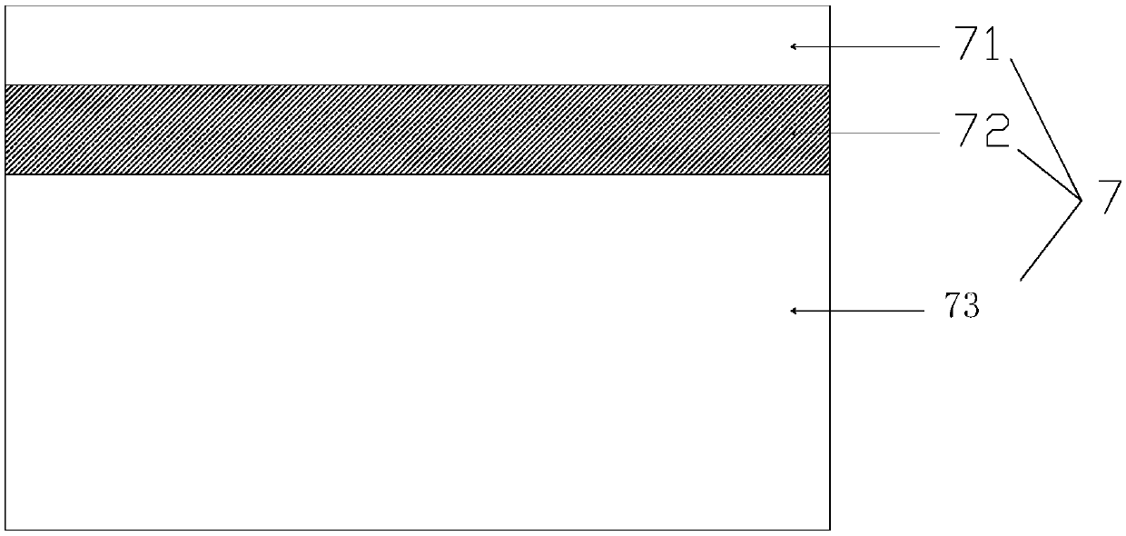
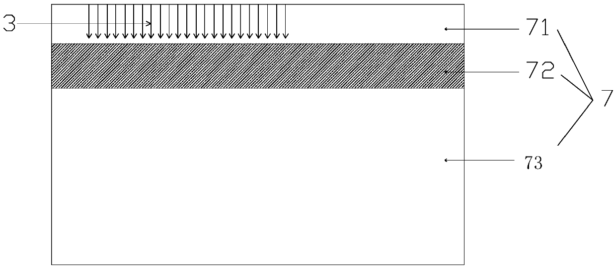
[0052] see Figure 7 and Figure 8 , a kind of thin film bulk acoustic resonator comprises SOI substrate 7, the lower electrode 3, piezoelectric layer 6 and top electrode 1 that are arranged on the first surface (front side) of SOI substrate 7 successively, on the second side of SOI substrate 7 The surface (back side) is provided with an air cavity 5, the depth of the air cavity is about 200 μm, and the area of ​​the air cavity is about 150 μm*150 μm; wherein the lower electrode 3 is the top layer silicon 71 of the SOI substrate 7 in the selected area after ion implantation The highly doped conductive silicon layer formed by the method conversion is also provided with a through hole 2 communicating with the outside world in the corresponding area between the piezoelectric layer 6 and the lower electrode 3; the air cavity 5 is arranged in the back substrate 73 of the SOI substrate 7; wherein The SOI substrate 7 includes a top layer of silicon 71 , a back substrate 73 and an ox...


PUM


Abstract

The invention discloses a film bulk acoustic resonator and a manufacturing method thereof. The manufacturing method comprises the steps of manufacturing a lower electrode on a first surface of an SOIsubstrate; forming a piezoelectric layer on the first surface of the SOI substrate and the lower electrode; forming a top electrode on the piezoelectric layer; and processing the second surface of theSOI substrate to form an air cavity, wherein the second surface and the first surface are arranged back to back. According to the manufacturing method provided by the invention, the preparation process of the FBAR is simplified, the AlN film crystal grown by the method is high in quality, the performance of the device is improved, and the frequency of the resonator is adjusted by controlling thethickness of top silicon through the position of silicon oxygen injection isolation; and the SOI material has the characteristics of low power consumption, high integration density, radiation resistance and the like, so that the complexity of a device preparation process is reduced, and the film bulk acoustic resonator is applicable to a radio frequency front end of a future 5G communication system.

Description

technical field [0001] The invention particularly relates to a film bulk acoustic wave resonator and a manufacturing method thereof, belonging to the technical field of communication electronic components. Background technique [0002] In 2017, domestic smartphone shipments reached 461 million units. Resonators are the core components of duplexers and filters that are widely used in mobile phone radio frequency devices; and with the development of communication, the number of compatible communication bands in mobile phones is increasing, and the number of resonators required is also gradually increasing. Wireless The development trend of multifunctional and integrated communication systems and the increase in the number of devices have put forward requirements for resonators such as miniaturization, integration, high frequency, and high performance; traditional microwave resonators use electromagnetic waves as carriers. The application of the communication frequency band re...

Claims


Application Information

Patent Timeline
Patent Type & Authority Applications(China)
IPC IPC(8): H03H9/17H03H3/02
CPCH03H9/171H03H9/173H03H3/02H03H2003/023H03H9/174H03H9/02015H03H9/02031H03H9/176
Inventor 张晓东于伦林文魁张宝顺
Owner SUZHOU INST OF NANO TECH & NANO BIONICS CHINESE ACEDEMY OF SCI
Why Eureka
Try Eureka