Stacked packaging structure and preparation method thereof

A technology of packaging structure and plastic packaging layer, which is applied in semiconductor/solid-state device manufacturing, electrical components, and electrical solid-state devices, etc., can solve problems such as increased process difficulty, negative impact on the overall reliability of the package, and increased cost.

Inactive Publication Date: 2020-04-07
江苏中科智芯集成科技有限公司
View PDF4 Cites 6 Cited by
  • Summary
  • Abstract
  • Description
  • Claims
  • Application Information

AI Technical Summary

Problems solved by technology

However, since the large-sized channel can satisfy the function of conductive interconnection after being filled to a certain thickness, the method of electroplating copper is still used to completely fill the channel, which not only increases the cost, but also makes the process more difficult. Filled, the middle of the conductive channel is still empty, the residual material in the process flow, or the reactants generated will accumulate in the middle of the channel, which will have a serious negative impact on the overall reliability of the package

Method used


Image

  • Stacked packaging structure and preparation method thereof
  • Stacked packaging structure and preparation method thereof
  • Stacked packaging structure and preparation method thereof

Examples


Embodiment Construction

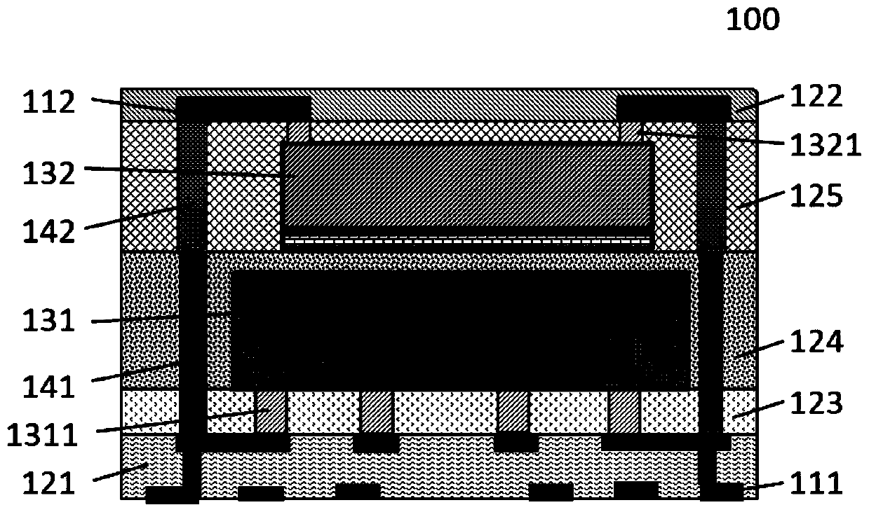
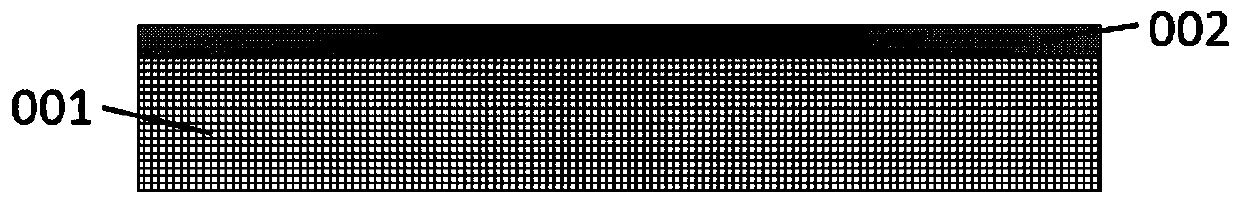
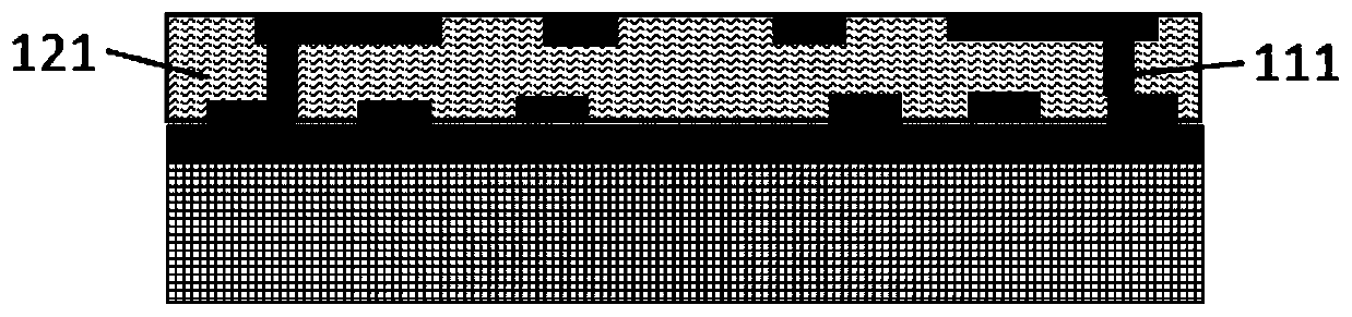
[0059] In the following description, the present invention is described with reference to various examples. One skilled in the art will recognize, however, that the various embodiments may be practiced without one or more of the specific details, or with other alternative and / or additional methods, materials, or components. In other instances, well-known structures, materials, or operations are not shown or described in detail so as not to obscure the inventive concepts of the present invention. Similarly, for purposes of explanation, specific quantities, materials and configurations are set forth in order to provide a thorough understanding of embodiments of the invention. However, the invention is not limited to these specific details. Furthermore, it should be understood that the embodiments shown in the drawings are illustrative representations and are not necessarily drawn to correct scale.

[0060] In this specification, reference to "one embodiment" or "the embodiment...


PUM

PropertyMeasurementUnit
thicknessaaaaaaaaaa

Abstract

The invention discloses a stacked packaging structure, which comprises: a first chip, wherein the first chip is inversely attached to the first rewiring layer, and a welding pad of the first chip is provided with a bump; a bottom layer filling film covering the front surface of the first chip; a first conductive channel disposed around the first chip; a first plastic package layer wrapping the first chip and the upper part of the first conductive channel; the first rewiring layer which is formed on the back surface of the bottom layer filling film and is electrically connected to the first chip and the first conductive channel; a first dielectric layer covering the surface and a gap of the first rewiring layer; a second chip right attached to the surface of the first plastic package layer;a second conductive channel disposed around the second chip; a second plastic package layer wrapping the second chip and the second conductive channel; a second rewiring layer formed on the surface of the second plastic package layer and electrically connected to the second chip and the second conductive channel; and a second dielectric layer covering the surface and a gap of the second redistribution layer.

Description

technical field [0001] The invention relates to the technical field of semiconductor integrated circuit packaging, in particular to a stack packaging technology. Background technique [0002] With the rapid development of semiconductor integrated circuit technology, electronic packaging products have a high-density, multi-functional development trend. Three-dimensional stack packaging means that at least two layers of chips are stacked and packaged, so that more semiconductor chips can be integrated in a smaller space. In the prior art, vertical conductive channels and rewiring structures are often used to realize the conductive interconnection of chips of each layer. When the diameter of the channel is small, methods such as atomic layer deposition (ALD) and chemical vapor deposition (CVD) can be used to first deposit the metal adhesion layer and seed layer, or only deposit the conductive metal adhesion layer, and then electroplate copper to fill the conductive channel . ...

Claims


Application Information

Patent Timeline
Patent Type & Authority Applications(China)
IPC IPC(8): H01L23/538H01L23/31H01L21/56H01L21/768
CPCH01L21/56H01L21/76885H01L21/76895H01L21/76897H01L23/3114H01L23/5384H01L23/5386H01L2224/16225H01L2224/18
Inventor 姚大平
Owner 江苏中科智芯集成科技有限公司
Why Eureka
Try Eureka