Method for improving layout photoetching performance, corrected layout and simulation method

A performance and lithography technology, which is applied in the direction of microlithography exposure equipment, originals for photomechanical processing, photolithography process exposure devices, etc., can solve the problem of poor lithography quality, smaller layout process window, and inability to effectively suppress Prohibition of periodical effects, dense periodical lines, mutual restriction and other issues, to achieve the effect of low cost, improved lithography quality, and improved lithography performance

Pending Publication Date: 2020-04-10
INST OF MICROELECTRONICS CHINESE ACAD OF SCI
View PDF5 Cites 3 Cited by
  • Summary
  • Abstract
  • Description
  • Claims
  • Application Information

AI Technical Summary

Problems solved by technology

[0005] In view of the above analysis, the present invention aims to provide a method for improving the performance of layout lithography, a revised layout and a simulation method to solve the problem that the existing process cannot effectively suppress the prohibition period effect and the mutual restriction of dense period lines. Traditional OPC ( Optical proximity effect correction) is difficult to solve in a balanced manner, resulting in a smaller process window of the entire layout and a significant deterioration in lithography quality

Method used


Image

  • Method for improving layout photoetching performance, corrected layout and simulation method
  • Method for improving layout photoetching performance, corrected layout and simulation method
  • Method for improving layout photoetching performance, corrected layout and simulation method

Examples


Embodiment 1

[0054] A specific embodiment of the present invention discloses a method for improving photolithography performance by optimizing a one-dimensional line pattern structure in which prohibited periods and dense periods are alternately arranged, including the following steps:

[0055] Step 1: Obtain an optimized free light source considering the global situation. Obtain various types of test patterns as comprehensive as possible from the actual layout as the initial layout input. Initial light source parameters (generally, a ring light source is used as the initial light source) and related simulation parameters include lithography machine model, NA (numerical aperture) value, mask plate parameters (thickness, refractive index, etc.), etc.;

[0056] Step 2: Under the above parameter settings, use professional simulation software to perform collaborative optimization of light source mask (SMO) to obtain the optimized free light source (freeform source1), and analyze the data to fi...

Embodiment 2

[0073] The resolution limit size of the 193nm immersion lithography technology is 76nm, and this embodiment uses a test pattern with a minimum period of 80nm. The simulation software uses the tachyon SMO function of ASML Brion to realize the optimization simulation of the light source mask.

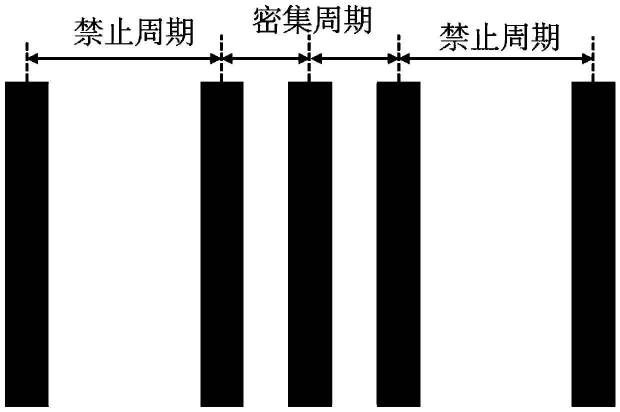
[0074] In the photolithography process, for the forbidden periodic pattern (forbidden pitch, FP), it can be solved by properly reducing the radius of the light source and sacrificing some critical dimensions of the process window. On the contrary, for small-sized key graphics, it can be solved by appropriately increasing the radius of the light source. Therefore, due to the competitive relationship between FP and critical dimension graphics, it is impossible to balance the graphics where the two situations coexist by modifying the light source at the same time, and the graphics that combine dense periodic lines and FP (FDA graphics, such as figure 1 shown) has become an extremely difficu...

Embodiment 3

[0096] A specific embodiment of the present invention discloses a method for finding out the lithography forbidden period (forbiddenpitch, FP) by calculation simulation, such as Figure 14 shown, including the following steps:

[0097] Step 1: Obtain a test pattern (test pattern), mainly a one-dimensional variable-period line (through pitch) pattern within a certain range, and the line width (critical dimension, CD) is the key line width (ie, key dimension) of the lithography node , for example, the actual key line width of the 14nm node is 38nm, and the period (pitch) should include as much as possible;

[0098] Step 2: Set initial simulation light source parameters (for example, a circular light source or a ring light source is used as the initial light source, and a ring light source is used as the initial light source in this embodiment) and related simulation parameters, such as the model of the lithography machine, NA (numerical aperture) value, Reticle parameters and p...


PUM


Abstract

The invention relates to a method for improving A layout photoetching performance, a corrected layout and a simulation method, and belongs to the technical field of semiconductor photoetching, and solves the problems that the process window of the whole layout is reduced and the photoetching quality is obviously reduced because the mutual restriction of a prohibition periodic effect and a dense periodic line cannot be effectively inhibited and the traditional OPC is difficult to balance and solve in the prior art. The method for improving the photoetching performance comprises the following steps of: obtaining a most representative graph in a graph category with remarkable influence on the photoetching performance through simulation; increasing the width of a forbidden period side edge single line; fixing the position of the middle line of a dense periodic line, and keeping the size of the middle line unchanged; and outwards widening the outer side edge edge3 of the side edge line of the dense periodic line by a certain distance delta edge3 to obtain an adjusted and corrected graph. According to the invention, the photoetching performance of the layout is improved with low cost andlow risk.

Description

technical field [0001] The invention relates to the technical field of semiconductor photolithography, in particular to a method for improving the performance of layout photolithography, a corrected layout and a simulation method. Background technique [0002] For lithography nodes below 20nm, especially 193nm immersion lithography, the size of lithography has almost reached the physical limit. Although many resolution enhancement techniques have been adopted, such as source mask collaborative optimization (SMO), optical proximity correction (OPC), or adding sub-resolution auxiliary graphics (Sbar), etc., due to some insurmountable problems, the process window However, the increase still faces great challenges, for example, the forbidden period (forbidden pitch, FP) effect. There will be some forbidden periods in lithography, that is, patterns within this size range will cause the process window of the entire layout to become smaller, and the quality of lithography will be ...

Claims


Application Information

Patent Timeline
IPC IPC(8): G03F1/72G03F7/20
CPCG03F1/72G03F7/70491G03F7/705
Inventor 何建芳韦亚一董立松张利斌陈睿张双
Owner INST OF MICROELECTRONICS CHINESE ACAD OF SCI
Why Eureka
Try Eureka