Photovoltaic SE battery and preparation method thereof
A battery and photovoltaic technology, applied in the field of solar cells, can solve the problems of high cost of raw materials for silicon-based solar cells, high cost of production equipment, complex preparation process, etc., and achieve the effects of reducing reflectivity, improving service life, and reducing compounding.
- Summary
- Abstract
- Description
- Claims
- Application Information
AI Technical Summary
Problems solved by technology
Method used
Image
Examples
Embodiment 1
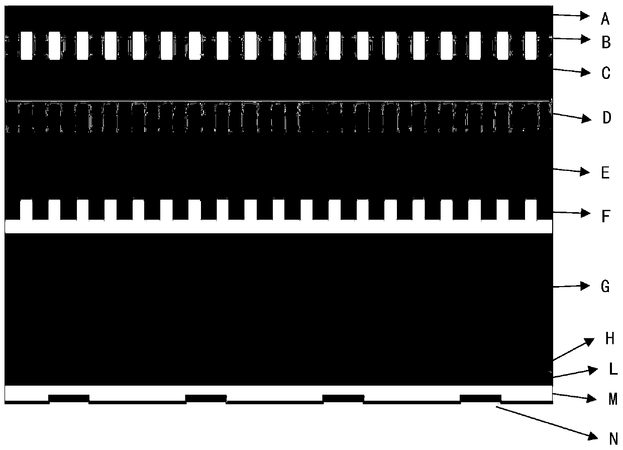
[0068] Embodiment 1 of the present invention discloses a photovoltaic SE battery, including a back field electrode, a back electrode, a protective film, a passivation layer, a P-type silicon substrate, a PN junction layer, an SE laser propulsion layer, an oxidation repair layer, and an antireflection film layer , auxiliary grid electrode and main grid electrode;
[0069] On one side of the P-type silicon substrate, a PN junction layer and an SE laser propelling layer are sequentially grown, and the PN junction layer and the SE laser propelling layer form a plurality of parallel first grooves on the contact surface;
[0070] A passivation layer is arranged on the other side of the P-type silicon substrate, the outer surface of the passivation layer is connected to a protective film, a back electrode is arranged outside the protective film, and a back field electrode is arranged on the outer surface of the back electrode;
[0071] The SE laser propelling layer forms a plurality ...
Embodiment 2
[0102] Embodiment 2 of the present invention discloses a method for preparing a photovoltaic SE battery as disclosed in Embodiment 1, which specifically includes the following steps:
[0103] (1) Wash and make texture on one side of the P-type silicon substrate to form a textured layer, and diffuse on the surface of the textured layer to form a PN junction layer; the P-type silicon substrate is a square monocrystalline silicon wafer with a side length of 156.75-210 mm, The thickness is 180±20μm; the thinning amount of washing and making texture is 0.38~0.58g;
[0104] (2) Laser propulsion is carried out on the surface of the PN junction layer to form an SE laser propulsion layer; the propulsion depth of the laser propulsion is 0.1-0.15 μm, the length of the groove line formed by the propulsion is 155.25 mm, and the line width is 80-120 μm;
[0105] (3) Perform low-temperature annealing treatment on the SE laser propelling layer, and then perform high-temperature thermal oxygen...
Embodiment 3
[0114] Embodiment 3 of the present invention discloses a method for preparing a photovoltaic SE battery as disclosed in Embodiment 1, which specifically includes the following steps:
[0115] (1) Choose a 156.75x156.75mm single crystal silicon wafer with a thickness within the range of 180±20μm; clean the silicon wafer before making texture, remove the loss layer and impurities of the original wafer itself, and form a texture layer, in which the amount of thinning is controlled It is 0.4g; then it is placed in a diffusion device for diffusion junction to form a PN junction layer, and its surface resistance is between 125Ω.
[0116] (2) Carry out laser propulsion on the surface of the PN junction layer of the above-mentioned diffused single crystal silicon wafer, the propelling depth is 0.05 μm, the length of the groove line formed by propelling is 156.75 mm, and the line width is between 118 μm.
[0117] (3) Perform oxidation repair on the above-mentioned single crystal silico...
PUM
| Property | Measurement | Unit |
|---|---|---|
| Thickness | aaaaa | aaaaa |
| Thickness | aaaaa | aaaaa |
| Width | aaaaa | aaaaa |
Abstract
Description
Claims
Application Information

