
Method for manufacturing monocrystalline silicon SE-PERC battery through secondary annealing

A technology of an infrared laser and a manufacturing method, applied in the field of solar cells, can solve the problems of reducing the photoelectric conversion efficiency, damage, open voltage and short-circuit current of crystalline silicon cells of a single crystal silicon SE-PERC cell, and reduce carriers. Compounding, improving open pressure and short flow, repairing the effect of damage

Inactive Publication Date: 2020-04-10
ZHEJIANG AIKO SOLAR ENERGY TECH CO LTD
View PDF6 Cites 0 Cited by
  • Summary
  • Abstract
  • Description
  • Claims
  • Application Information

AI Technical Summary

Problems solved by technology

[0014] As far as monocrystalline silicon SE-PERC cells are concerned, during the process of selecting the emitter through the front laser step, the laser energy is in the form of a Gaussian distribution, and relatively heavy damage will occur in the area where the laser acts, which will destroy the original The lattice structure of the textured surface of the silicon wafer makes the carriers recombine near the surface defect state, which leads to the decrease of the opening voltage and short current of the crystalline silicon cell, and reduces the photoelectric conversion efficiency of the monocrystalline silicon SE-PERC cell

Method used


Image

  • Method for manufacturing monocrystalline silicon SE-PERC battery through secondary annealing
  • Method for manufacturing monocrystalline silicon SE-PERC battery through secondary annealing
  • Method for manufacturing monocrystalline silicon SE-PERC battery through secondary annealing

Examples


Embodiment Construction

[0023] The specific implementation manners of the present invention will be further described in detail below in conjunction with the accompanying drawings and embodiments. The following examples are used to illustrate the present invention, but are not intended to limit the scope of the present invention.

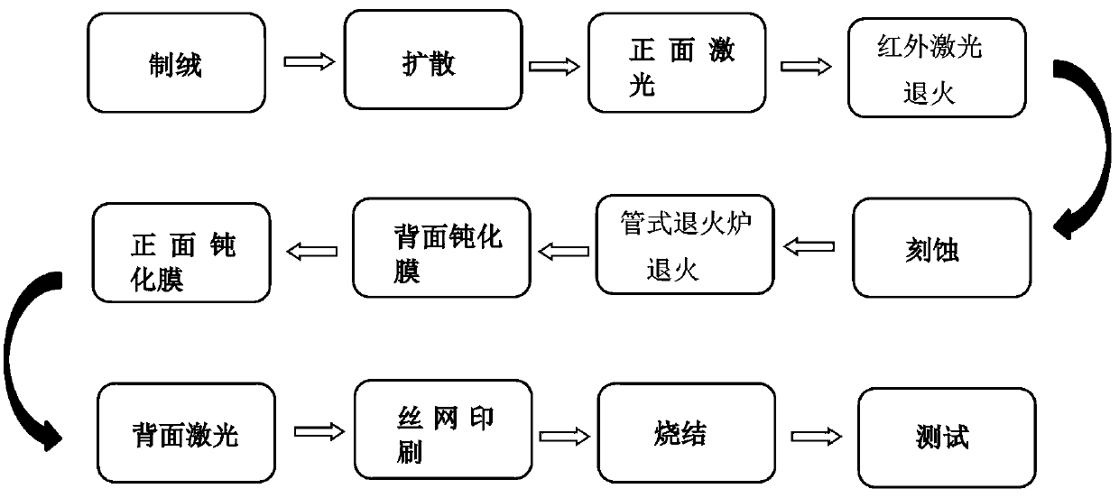
[0024] Such as Figure 1~2 Shown, a kind of manufacturing method of the monocrystalline silicon SE-PERC cell of infrared laser annealing, the step comprises:

[0025] 1. Texture making: use wet technology to form a textured surface on the surface of the P-type monocrystalline silicon wafer;

[0026] 2. Diffusion: P-N junction is formed by diffusion;

[0027] 3. Front laser: Prepare selective emitter, and use laser to do heavy doping on the surface of silicon wafer;

[0028] 4. Infrared laser annealing: Repair the damage caused by the front laser to the surface of the silicon wafer, passivate the surface to reduce the recombination of carriers.

[0029] 5. Etching: use ...


PUM


Abstract

The invention discloses a method for manufacturing a monocrystalline silicon SE-PERC battery through secondary annealing, and the method comprises the steps: texturing, diffusion, front laser, etching, annealing, rear surface passivation of a film, front surface passivation of a film, back laser, silk-screen printing, sintering, and testing, and is characterized in that a step of repairing damageannealing is added after the front laser step and before the etching step. A laser annealing step is carried out after the front laser step, and a silicon wafer is put into a tubular annealing furnaceto be annealed, so that the effect of repairing damage of the front laser to the surface of the silicon wafer is achieved, the surface is passivated, carrier recombination is reduced, and the open-circuit voltage and the short-circuit current of a crystalline silicon cell are improved.

Description

technical field [0001] The invention relates to the technical field of solar cells, in particular to a method for manufacturing an infrared laser annealed single crystal silicon SE-PERC cell. Background technique [0002] With the rise of monocrystalline silicon SE-PERC cells, lasers are more widely used in the preparation of crystalline silicon cells. Laser slotting and selective emitter preparation are inseparable from lasers. Technologies such as Metal Wrap Back Contact (MWT) and Emitter Piercing (EWT) also require laser perforation. The traditional monocrystalline silicon SE-PERC cell manufacturing steps are: [0003] 1. Texture making: use wet technology to form a textured surface on the surface of the P-type monocrystalline silicon wafer; [0004] 2. Diffusion: P-N junction is formed by diffusion; [0005] 3. Front laser: Prepare selective emitter, and use laser to do heavy doping on the surface of silicon wafer; [0006] 4. Etching: use HF / HNO3 solution for back...

Claims


Application Information

Patent Timeline
IPC IPC(8): H01L31/18
CPCH01L31/1804Y02P70/50
Inventor 韩大伟林纲正陈刚
Owner ZHEJIANG AIKO SOLAR ENERGY TECH CO LTD
Features
  • Generate Ideas
  • Intellectual Property
  • Life Sciences
  • Materials
  • Tech Scout
  • Unparalleled Data Quality
  • Higher Quality Content
  • 60% Fewer Hallucinations
Learn More