Organic compound, electronic device, and electronic apparatus

An organic compound and chemical formula technology, applied in the field of organic compounds, can solve the problems of high driving voltage, low luminous efficiency, poor thermal stability, etc., and achieve the effects of low voltage, excellent hole transport performance, and high luminous efficiency

Inactive Publication Date: 2020-04-14
SHAANXI LIGHTE OPTOELECTRONICS MATERIAL CO LTD
View PDF1 Cites 4 Cited by
  • Summary
  • Abstract
  • Description
  • Claims
  • Application Information

AI Technical Summary

Problems solved by technology

[0004] However, there are still many problems in the current commercialized OLED devices, such as high driving voltage, low luminous efficiency, poor thermal stability, and short life, especially in blue OLED devices. Efficiency, high thermal stability, long life OLED devices and related materials have become the problems that have to be overcome in the field of organic electroluminescence

Method used


Image

  • Organic compound, electronic device, and electronic apparatus
  • Organic compound, electronic device, and electronic apparatus
  • Organic compound, electronic device, and electronic apparatus

Examples


Embodiment 1

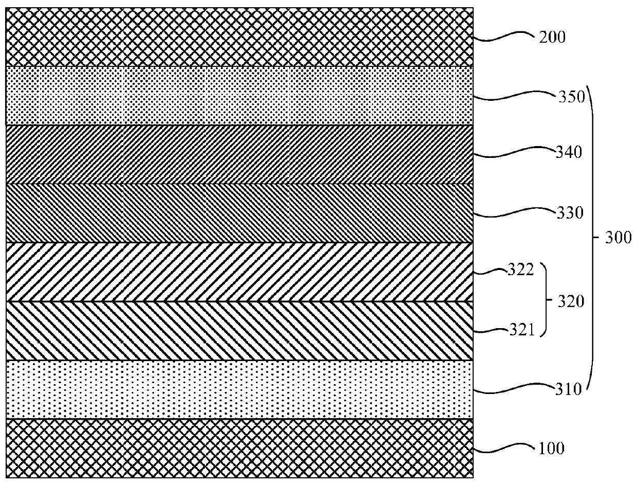
[0236] Organic electroluminescent devices using compound 1 as hole transport layer (HTL) material

[0237] Organic electroluminescent devices were prepared by the following process:

[0238] Set the ITO thickness to The ITO substrate (manufactured by Corning) was cut into a size of 40mm (length) × 40mm (width) × 0.7mm (thickness), and then it was prepared into an experiment with anode, cathode bonding area and insulating layer by photolithography process. Substrate (light-emitting pixel point size is 3mm×3mm), using ultraviolet ozone and O 2 :N 2Plasma surface treatment was performed to increase the work function of the anode (experimental substrate) and to remove scum.

[0239] 10 nm of HAT-CN (CAS No.: 105598-27-4) was evaporated as a hole injection layer (HIL) on the anode.

[0240] Next, a layer of Compound 1 of the present invention was vapor-deposited with a thickness of 100 nm to form a hole transport layer (HTL).

[0241] TCTA (CAS No.: 139092-78-7) was vacuum-ev...

Embodiment 2~15

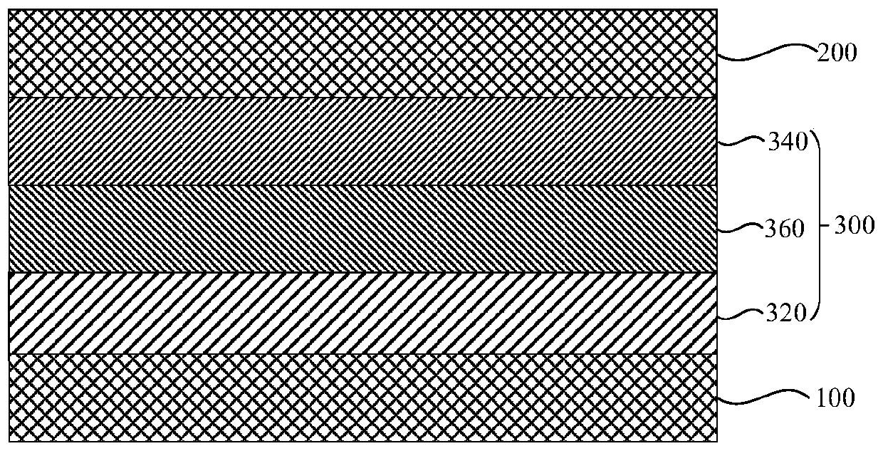
[0248] In the above device structure, in addition to replacing the compound 1 of the hole transport layer (HTL) with compounds 2, 3, 4, 5, 6, 7, 17, 21, 41, 49, 61, 87, 100, 122, implement Examples 2-15 used the same method as Example 1 to prepare organic electroluminescent devices.


PUM

PropertyMeasurementUnit
thicknessaaaaaaaaaa
thicknessaaaaaaaaaa

Abstract

The present application relates to an organic compound, an electronic device comprising the organic compound, and an electronic apparatus comprising the electronic device. The main body of the organiccompound is a fused heteroaromatic ring group containing fluorene or silafluorene, a large-plane structure is shown in a three-dimensional space, and an electron-rich aryl amine or heteroaryl amine substituent group is introduced to the ninth position of fluorene or silafluorene, so that the hole transport performance of the compound is excellent.

Description

technical field [0001] The present application relates to the technical field of organic compounds, in particular to an organic compound, an electronic device and an electronic device. Background technique [0002] An organic electroluminescent device (OLED: Organic Light Emitting device) is a self-luminous light-emitting device. The principle is that when an electric field is applied to the negative and positive poles, the holes on the anode side and the electrons on the cathode side will move to the light-emitting layer, and combine in the light-emitting layer to form excitons. The process of releasing energy for the ground state emits light outward. Therefore, it is crucial to improve the recombination of electrons and holes in OLED devices. [0003] In order to improve the brightness, efficiency and lifetime of organic electroluminescent devices, multilayer structures are often used in the devices. These multilayer structures include: hole injection layer, hole transp...

Claims


Application Information

Patent Timeline
Patent Type & Authority Applications(China)
IPC IPC(8): C07D319/14C07F7/10C07D409/04C07D327/06C07D407/04C07D405/14C07D409/12C07D401/12C07D471/04C07D407/12C07D401/04C07D409/14C07D405/10C07D411/10C07D411/14C07D339/08C07D411/04C07D411/12H01L51/50H01L51/54H01L51/42H01L51/46
CPCC07D319/14C07F7/0816C07F7/0812C07D409/04C07D327/06C07D407/04C07D405/14C07D409/12C07D401/12C07D471/04C07D407/12C07D401/04C07D409/14C07D405/10C07D411/10C07D411/14C07D339/08C07D411/04C07D411/12H10K85/615H10K85/626H10K85/654H10K85/657H10K85/6572H10K85/6574H10K85/6576H10K85/40H10K30/00H10K50/15Y02E10/549
Inventor 李健沙荀姗喻超
Owner SHAANXI LIGHTE OPTOELECTRONICS MATERIAL CO LTD
Why Eureka
Try Eureka