Inner layer manufacturing method of multilayer thick copper plate

A production method and technology of thick copper plates, which are applied in multilayer circuit manufacturing, printed circuit manufacturing, printed circuit, etc., can solve the problems of increased motor weight, reduced thermal conductivity, and increased air gap of the motor, and achieve reduced number of sheets and improved thermal conductivity. The effect of low and small kerf width

Active Publication Date: 2020-04-21
QINGSHENG AUTOMATION TECH SHANGHAI
View PDF6 Cites 4 Cited by
  • Summary
  • Abstract
  • Description
  • Claims
  • Application Information

AI Technical Summary

Problems solved by technology

When the number of PP sheets in the inner prepreg increases, the thermal conductivity of the inner layer of the finished PCB board decreases, and the heat conduction effect becomes worse, which limits the increase in the current of the device, thereby inhibiting the increase in device power; when the thickness of the finished PCB board after lamination increases After large, such as for the axial magnetic field ironless permanent magnet motor, the air gap of the motor increases
Therefore, in order to achieve the same magnetic field strength, more permanent magnet materials need to be used, the use of increased materials, and the weight of the motor also increases

Method used


Image

  • Inner layer manufacturing method of multilayer thick copper plate

Examples


Embodiment Construction

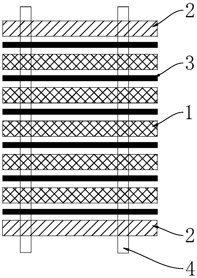
[0037] The implementation of the present invention will be illustrated by specific specific examples below, and those skilled in the art can easily understand other advantages and effects of the present invention from the contents disclosed in this specification.

[0038] It should be noted that the structures, proportions, sizes, etc. shown in the drawings attached to this specification are only used to match the content disclosed in the specification, for those who are familiar with this technology to understand and read, and are not used to limit the implementation of the present invention. Limiting conditions, so there is no technical substantive meaning, any modification of structure, change of proportional relationship or adjustment of size, without affecting the effect and purpose of the present invention, should still fall within the scope of the present invention. The disclosed technical content must be within the scope covered. At the same time, terms such as "upper"...


PUM


Abstract

The invention provides an inner layer manufacturing method of a multilayer thick copper plate, which comprises the steps of obtaining a copper foil plate, and carrying out surface treatment on the copper foil plate; carrying out pattern processing on the copper foil plate by adopting a laser cutting method to form a pre-compiled pattern; adding prepreg between two copper foil plates, and laminating the prepreg and the copper foil plates in sequence; and carrying out vacuum heating and press-fitting to form a laminated plate. According to the invention, the copper foil is cut by laser, and thekerf width is small, i.e., the line spacing between lines is small; chemical etching is not needed in laser cutting, and the whole process is environmentally friendly and free of pollution; meanwhile,the edges of the kerfs are smooth, the side etching phenomenon of chemical etching is avoided, the instantaneous current impact resistance of the coil is further enhanced, and the consistency of products is improved at the same time. In the copper foil cutting process, gaps are filled with resin for the kerfs, so that the local pattern can be prevented from falling off, and the stability of the pattern is enhanced on the one hand; and on the other hand, the gaps of the pattern are filled with resin in advance, the number of layers of prepreg in the press-fitting process can be reduced, and the plate thickness of a finished product is reduced.

Description

technical field [0001] The invention relates to the technical field of circuit boards, in particular to an inner layer manufacturing method of a multilayer thick copper board. Background technique [0002] In recent years, thick copper PCB boards have been widely used in power-related products, such as wireless chargers, planar transformers, and ironless stators for permanent magnet motors. The common feature of this kind of products is that the current is large when working, and the basic shape is relatively regular, which is generally a rotary coil; the thickness of the copper foil of the PCB double-sided copper clad laminate used is mostly not less than 4 ounces, 1 ounce = 0.035mm; at the same time, the PCB It is a high-rise board, and some layers have as many as 26 layers. [0003] In the traditional PCB production process, the inner layer adopts an etching process, using chemical potions to corrode the copper foil to generate graphics to achieve the purpose of processi...

Claims


Application Information

Patent Timeline
IPC IPC(8): H05K3/46
CPCH05K3/4632H05K2203/03H05K2203/107
Inventor 易旭
Owner QINGSHENG AUTOMATION TECH SHANGHAI
Why Eureka
Try Eureka