High-speed precision crystal silicon laser etching apparatus and method

A technology of laser etching and process method, which is applied in the direction of laser welding equipment, manufacturing tools, welding equipment, etc., can solve the problem that the production process of crystalline silicon cannot meet the development needs of solar energy technology, and achieve controllable processing graphics and processing paths, Effect of high precision and increased surface doping concentration

Inactive Publication Date: 2011-09-28
周明
View PDF5 Cites 30 Cited by
  • Summary
  • Abstract
  • Description
  • Claims
  • Application Information

AI Technical Summary

Problems solved by technology

[0005] In order to solve the problem that the production process of crystalline silicon in the prior art field proposed in the above-mentioned background technology cannot meet the needs of the development of solar energy technology, the present invention provides the following technical solutions:

Method used


Image

  • High-speed precision crystal silicon laser etching apparatus and method
  • High-speed precision crystal silicon laser etching apparatus and method

Examples


Embodiment Construction

[0031] The process embodiment will be described in detail below, so that the advantages and features of the present invention can be more easily understood by those skilled in the art, so as to define the protection scope of the present invention more clearly.

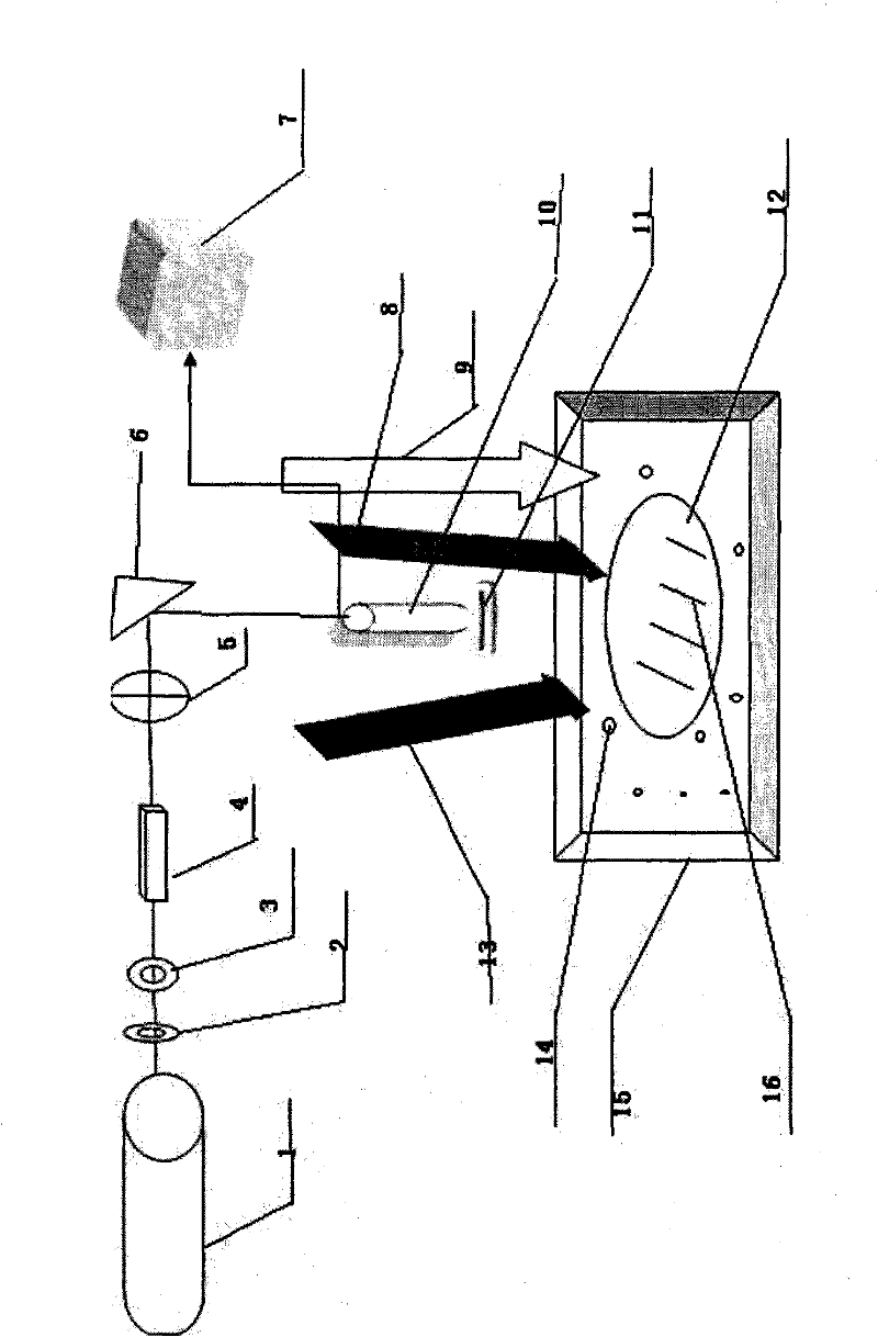
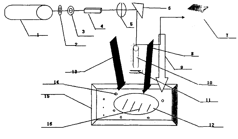
[0032] Such as figure 1 It is a schematic diagram of the structure of crystal silicon high-speed precision laser etching equipment. Before processing, the laser focus is on the upper surface of the silicon wafer. After the laser beam emitted by laser 1 passes through the shutter 2 and passes through the electric 1 / 2 filter 3, the beam can not be changed. If the polarization state is changed by 90 degrees, two kinds of vertical etching lines can be operated. After the laser beam enters the coaxial beam expander 4, the laser beam can be expanded to achieve what is required in the specially customized three-dimensional dynamic focusing galvanometer system 10. The required light incident diameter and beam divergence angle ...


PUM


Abstract

The invention provides a high-speed precision crystal silicon laser etching apparatus and method. The method comprises the following steps: (A) placing a single crystal silicon wafer or a polycrystalline silicon wafer on a four-dimensional precision moving platform for laser processing by using a specific manipulator, with the aid of an observation and monitoring CCD system; (B) precisely focusing a laser beam on the surface of the silicon wafer, scanning the surface of the silicon wafer at a high speed by using a three-dimensional dynamic focusing vibration mirror in cooperation with a specific telecentric field lens, rising the surface etching temperature of the silicon wafer, and feeding phosphorous paste or phosphoric acid to a high-speed laser etching line at the same time; and (C) removing the manipulator for the silicon wafer and fixing next silicon wafer at the same time, and repeating the above drilling mode at. The method has the following advantages: laser has the characteristics of non-contact, no environment pollution and easy controllability, and can achieve the automatic control; since the laser focusing spot is in a micrometer size or smaller, thereby achieving high silicon wafer etching accuracy, small heat affected zone at the edge, and little damage to the substrate; and the power generation efficiency of the crystal silicon is further improved, and the production cost is further reduced.

Description

technical field [0001] The invention belongs to the fields of laser micro-nano processing, solar photovoltaic and semiconductor manufacturing, and in particular relates to equipment and a process method for high-speed and precise laser etching of crystalline silicon. Background technique [0002] Solar power generation is considered to be the most important new energy source in the 21st century due to its characteristics of no pollution, safety, simple maintenance, and inexhaustible resources, and it occupies more than 80% of the world's photovoltaic market. Crystalline silicon solar cells are widely used in solar rooftop power stations, commercial power stations and urban power stations with high land costs. They are currently the most mature and widely used solar photovoltaic products. And as the price of crystalline silicon continues to hit new lows, the cost of crystalline silicon solar cells will also drop significantly. Crystalline silicon cells have the characteristic...

Claims


Application Information

Patent Timeline
Patent Type & Authority Applications(China)
IPC IPC(8): H01L31/18B23K26/36B23K26/42B23K26/02B23K26/362B23K26/60
Inventor 周明
Owner 周明
Why Eureka
Try Eureka