Sputtering system and method for forming a metal layer on a semiconductor device

A semiconductor and device layer technology, applied in the field of sputtering process, can solve the problems of increasing the difficulty of step coverage and reducing the reliability of semiconductor devices, etc.

Pending Publication Date: 2020-04-21
GENERAL ELECTRIC CO
View PDF7 Cites 0 Cited by
  • Summary
  • Abstract
  • Description
  • Claims
  • Application Information

AI Technical Summary

Problems solved by technology

However, reducing cell size may cause challenges in the fabrication of semiconductor devices and their associated cells
In particular, as the cell size decreases, the size of trenches and openings in the stepped surface of semiconductor devices generally decreases, which may increase the difficulty in obtaining sufficient step coverage, thereby reducing the reliability of semiconductor devices.

Method used


Image

  • Sputtering system and method for forming a metal layer on a semiconductor device
  • Sputtering system and method for forming a metal layer on a semiconductor device
  • Sputtering system and method for forming a metal layer on a semiconductor device

Examples


Embodiment Construction

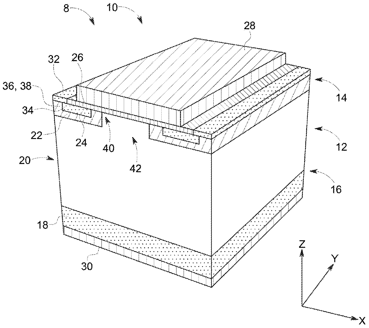
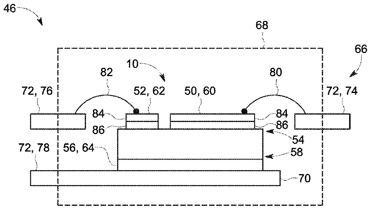
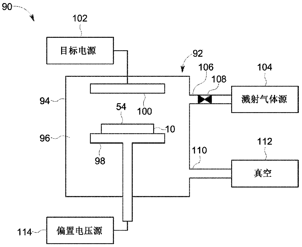
[0019] One or more specific embodiments are described below. In an effort to provide a concise description of these embodiments, not all features of an actual implementation are described in the specification. It should be understood that in the development of any such actual implementation, such as in any engineering or design project, a number of implementation-specific decisions must be made in order to achieve the developer's specific goals, such as complying with system-related and business-related constraints, which may vary from one implementation to another. In addition, it should be understood that such a development effort might be complex and time consuming, but would nevertheless be a routine undertaking of design, production, and manufacture for those of ordinary skill having the benefit of this disclosure.

[0020] Unless defined otherwise, technical and scientific terms used herein have the same meaning as commonly understood by one of ordinary skill in the art...


PUM

PropertyMeasurementUnit
Thicknessaaaaaaaaaa

Abstract

A method for sputtering an aluminum layer on a surface of a semiconductor device is presented. The method includes three sputtering steps for depositing the aluminum layer, where each sputtering stepincludes at least one sputtering parameter that is different from a corresponding sputtering parameter of another sputtering step. The surface of the semiconductor device includes a dielectric layer having a plurality of openings formed through the dielectric layer.

Description

technical field [0001] The subject matter disclosed herein relates to semiconductor devices, and more particularly, to sputtering processes for forming metal layers on semiconductor devices. Background technique [0002] Power conversion devices are widely used throughout modern power systems to convert electricity from one form to another for consumption by a load. Many power electronic systems utilize various semiconductor devices and components such as thyristors, diodes, and various types of transistors (e.g., metal-oxide-semiconductor field-effect transistors (MOSFETs), insulated-gate bipolar transistors (IGBTs) and other suitable transistors). Some semiconductor devices may include a plurality of cells (eg, transistor cells) formed on a semiconductor substrate. During fabrication of such semiconductor devices, one or more metal layers (eg, metallization) may be deposited on the surface of the semiconductor device to electrically connect features of the semiconductor ...

Claims


Application Information

Patent Timeline
IPC IPC(8): H01L29/772H01L21/8234H01L29/66H01L21/768H01L21/02
CPCH01L21/0485C23C14/165C23C14/025C23C14/345H01L21/76877H01L21/2855H01L23/485H01L23/53214H01L2224/48463H01L2224/48465H01L2924/181H01L2224/48247H01L2224/73265H01L2224/0603H01L2924/00012H01L21/02697H01L21/049H01L23/53223H01L21/28568
Inventor 斯泰西·乔伊·肯纳利维克多·托里斯戴维·利林菲尔德罗伯特·德韦恩·戈斯曼格雷戈里·基思·杜多夫
Owner GENERAL ELECTRIC CO
Why Eureka
Try Eureka