Check patentability & draft patents in minutes with Patsnap Eureka AI!

Pixel circuit, display panel and compensation method for reference voltage of pixel circuit

一种像素电路、电源电压的技术,应用在像素电路,像素电路基准电压的补偿领域,能够解决显示不均匀、薄膜晶体管电性漂移、面板发光不均匀等问题,达到发光均匀的效果

Inactive Publication Date: 2020-04-24
SHENZHEN CHINA STAR OPTOELECTRONICS SEMICON DISPLAY TECH CO LTD
View PDF8 Cites 0 Cited by
  • Summary
  • Abstract
  • Description
  • Claims
  • Application Information

AI Technical Summary

Problems solved by technology

However, as the panel is used for a longer period of time, the electrical properties of thin film transistors and OLEDs will drift, and eventually fail due to problems such as uneven display.
[0003] like figure 1 As shown, the pixel circuit of the traditional active matrix organic light emitting diode (AMOLED) is 3T1C. When the Data signal is written to the node G point stage, when the gate of T2 is closed, due to the coupling of the capacitor C1 The effect causes the voltage at point G to drop, causing the current flowing through T1 to change (such as figure 2 In the mark 10, there is a fluctuation in the current curve climb), and the coupling effect of different positions of the panel is different, resulting in uneven light emission of the panel

Method used


Image

  • Pixel circuit, display panel and compensation method for reference voltage of pixel circuit
  • Pixel circuit, display panel and compensation method for reference voltage of pixel circuit
  • Pixel circuit, display panel and compensation method for reference voltage of pixel circuit

Examples


Embodiment Construction

[0025] In order to better understand the content of the present invention, the present invention will be further illustrated by specific examples below, but the implementation and protection scope of the present invention are not limited thereto.

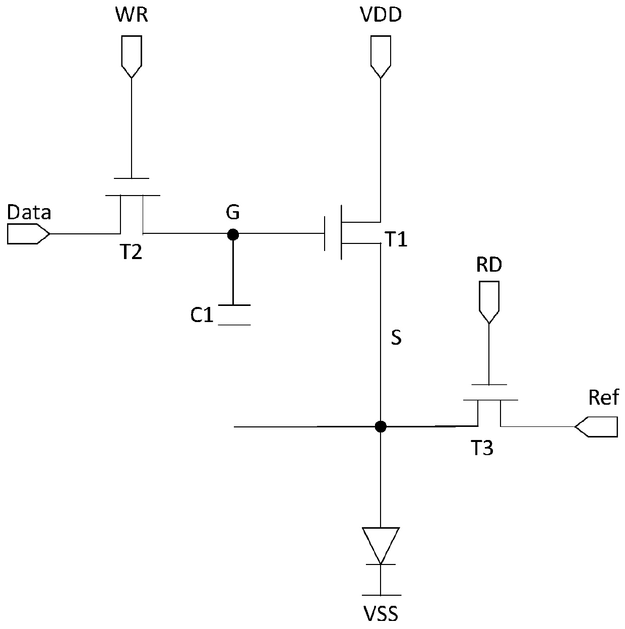
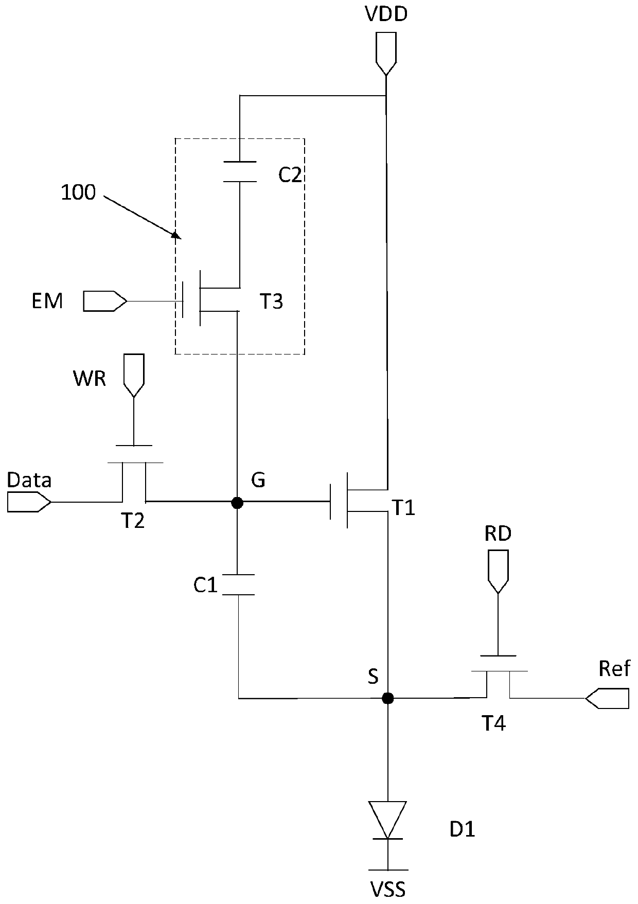
[0026] Such as image 3 As shown, the present invention provides a pixel circuit including a plurality of pixel internal driving circuits arranged in an array.

[0027] The internal driving circuit of each pixel includes: a first thin film transistor (T1), a second thin film transistor (T2), a fourth thin film transistor (T4), a first capacitor (C1), an organic light emitting diode (D1) and a compensation module.

[0028] The gate of the first thin film transistor (T1) is electrically connected to the first node (G), the source of the first thin film transistor is electrically connected to the second node (S), and the drain of the first thin film transistor Connect the power supply voltage (VDD).

[0029] The gate of the second thin film tr...


PUM


Abstract

The invention provides a pixel circuit, a display panel and a compensation method for reference voltage of the pixel circuit. The pixel circuit comprises a plurality of pixel internal driving circuitswhich are arranged in an array mode. Each pixel internal driving circuit comprises a first thin film transistor (T1), a second thin film transistor (T2), a fourth thin film transistor (T4), a first capacitor (C1), an organic light emitting diode (D1) and a compensation module. A compensation module is arranged. A scanning signal (EM) is accessed into the compensation module; one end of the compensation module is connected with a first node (G); and the other end thereof is connected with a power supply voltage (VDD) so as to compensate the potential drop of the first node (G) caused by the coupling of the first capacitor (C1), so that the reference voltage Vgs is kept unchanged, the current flowing through the driving thin film transistor (namely the first thin film transistor) is not changed, and the panel emits light uniformly.

Description

Technical field [0001] The present invention relates to the field of display technology, in particular to a pixel circuit, a display panel and a method for compensating the reference voltage of the pixel circuit. Background technique [0002] Organic light emitting diode (OLED) is a self-luminous display technology that has the advantages of wide viewing angle, high contrast, low power consumption, and bright colors. Due to these advantages, the proportion in the display industry is increasing year by year. Oxide thin film transistors are widely used in large-size AMOLEDs due to the advantages of high mobility and good uniformity. However, as the use time of the panel is prolonged, the electrical properties of the thin film transistor and OLED will drift, and eventually become invalid due to problems such as uneven display. [0003] Such as figure 1 As shown, the pixel circuit of the traditional active matrix organic light emitting diode (AMOLED) is 3T1C. When the Data signal is ...

Claims


Application Information

Patent Timeline
Patent Type & Authority Applications(China)
IPC IPC(8): G09G3/3225
CPCG09G3/3225G09G2300/0852G09G2300/0819G09G3/3233G09G2310/08H10K59/1213G09G3/3258G09G3/3266G09G2300/043G09G2300/0876
Inventor 肖翔薛炎
Owner SHENZHEN CHINA STAR OPTOELECTRONICS SEMICON DISPLAY TECH CO LTD
Features
  • R&D
  • Intellectual Property
  • Life Sciences
  • Materials
  • Tech Scout
  • Unparalleled Data Quality
  • Higher Quality Content
  • 60% Fewer Hallucinations
Learn More