Nanometer cold cathode electron source of coplanar double-gate focusing structure and manufacturing method of nanometer cold cathode electron source

A technology of focusing structure and cold cathode, which is applied in cold cathode manufacturing, electrode system manufacturing, discharge tube/lamp manufacturing, etc. Spotting, solving divergence, improving the effect of gate control characteristics

Active Publication Date: 2020-04-28
SUN YAT SEN UNIV
View PDF16 Cites 2 Cited by
  • Summary
  • Abstract
  • Description
  • Claims
  • Application Information

AI Technical Summary

Problems solved by technology

However, this structure does not fully utilize the cold cathode of the nanowires, that is, only the nanowires outside the growth source film are regulated by the gate, and the bottom ring electrode has a weak gate control effect and may also cause the divergence of the electron beam.

Method used


Image

  • Nanometer cold cathode electron source of coplanar double-gate focusing structure and manufacturing method of nanometer cold cathode electron source
  • Nanometer cold cathode electron source of coplanar double-gate focusing structure and manufacturing method of nanometer cold cathode electron source
  • Nanometer cold cathode electron source of coplanar double-gate focusing structure and manufacturing method of nanometer cold cathode electron source

Examples


Embodiment 1

[0049] This example prepares ZnO nanometer cold cathode electron source

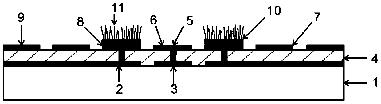
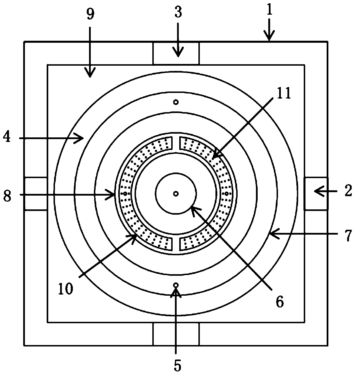
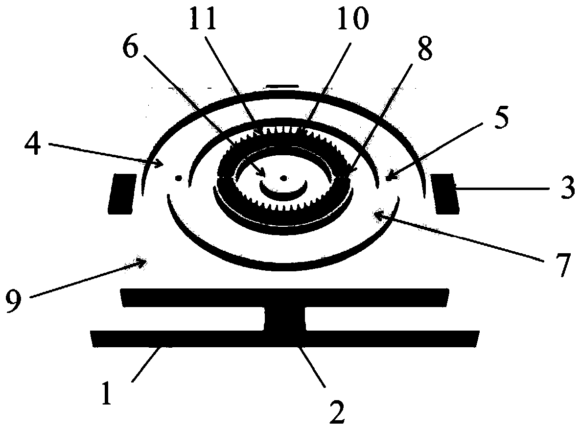
[0050] Such as Figure 1-Figure 3 As shown, the nano-cold cathode electron source of the coplanar double-gate focusing structure of the present invention includes a substrate 1, a bottom segmented cathode electrode 2, a bottom gate electrode 3, an insulating layer 4, an etched via hole 5, and a top layer internal gate Electrode 6, top-layer external ring-shaped gate electrode 7, top-layer ring-shaped cathode electrode 8, focusing electrode 9, growth source film 10, nanowire cold cathode 11.

[0051] There are two bottom segmented cathode electrodes 2 located on both sides of the bottom grid electrode 3 , and the outer leads of the bottom segment cathode electrodes 2 and the bottom grid electrode 3 are vertically arranged. The insulating layer 4 covers the bottom segmented cathode electrode 2 and the bottom grid electrode 3, and the insulating layer 4 is respectively etched with a number of etching throu...

Embodiment 2

[0061] The nano-cold cathode electron source array of the coplanar double-gate focusing structure in this embodiment is basically the same as that in Embodiment 1, as Figure 5 As shown, the difference is that the bottom grid electrodes form electrodes arranged in columns, and the segmented cathode electrodes on the bottom layer form electrodes arranged in rows under the connection of the ring-shaped cathode electrodes on the bottom layer. The design can make the bottom segmented cathode electrode and the bottom gate electrode perpendicular to each other on the same plane, so that the electron source array composed of the electron source has row and column addressing capability. The electron sources arranged in an array can repel the emitted electron beams by applying a negative voltage to the focusing electrode to produce a focusing effect, thereby realizing the micro-focus spot of the electron source.

Embodiment 3

[0063] The nano-cold cathode electron source of the coplanar double-gate focusing structure is basically the same as that of Embodiment 1, the difference is that

[0064] (1) The cathode substrate 11 is a large-area silicon wafer.

[0065] (2) The bottom segmented cathode electrode 2 and the bottom gate electrode 3 are made of Al, and the thickness range is 1 μm.

[0066] (3) The insulating film as the insulating layer 13 is composed of a silicon nitride insulating film; the thickness of the insulating layer is 1 μm;

[0067] (4) The top inner grid electrode 6, the top outer annular grid electrode 7, the top annular cathode electrode 8, and the focusing electrode 9 are made of AZO, and the thickness range is 2 μm;

[0068] (5) On the top ring-shaped cathode electrode 8, photolithographically locate the growth region of the nanowire cold cathode 11, and then deposit the growth source film 10; the growth source film 10 is molybdenum, and its thickness is 2.5 μm; the growth sour...


PUM

PropertyMeasurementUnit
thicknessaaaaaaaaaa
thicknessaaaaaaaaaa
thicknessaaaaaaaaaa

Abstract

The invention discloses a nanometer cold cathode electron source of a coplanar double-gate focusing structure, which comprises a substrate, an insulating layer, a bottom-layer segmented cathode electrode, a bottom-layer gate electrode, an etching through hole, a top-layer annular cathode electrode, a top-layer internal gate electrode, a top-layer external annular gate electrode, a growth source thin film, a nanowire cold cathode and a focusing electrode, wherein the top-layer internal gate electrode and the top-layer external annular gate electrode are connected with the bottom-layer gate electrode through the etching through hole, and the top-layer annular cathode electrode is connected with the bottom-layer segmented cathode electrode through the etching through hole. The invention further discloses a preparation method of the nanometer cold cathode electron source of the coplanar double-gate focusing structure. The nanometer cold cathode electron source has strong gate-control electron emission capability and electron beam focusing capability and has a coplanar double-gate focusing structure capable of row and column addressing.

Description

technical field [0001] The invention relates to the technical field of vacuum microelectronic devices, in particular to a nanometer cold cathode electron source with a coplanar double-gate focusing structure and a manufacturing method thereof. Background technique [0002] Chinese patent 201910834161.3, titled a nano-cold cathode electron source with a double ring gate structure and its manufacturing method, introduces the bottom segmented ring-shaped gate electrode and connects it with the top ring-shaped gate electrode by etching through holes, thereby Realize the series connection of the bottom ring-shaped gate electrodes to form the bottom ring-shaped electrodes, and form a double-ring gate structure with the top ring-shaped gate electrodes. However, this structure does not make full use of the nanowire cold cathode, that is, only the nanowires outside the growth source film are regulated by the gate, and the bottom ring electrode has a weak gate control effect and may a...

Claims


Application Information

Patent Timeline
Patent Type & Authority Applications(China)
IPC IPC(8): H01J1/304H01J1/02H01J9/02
CPCH01J1/02H01J1/304H01J9/02H01J9/025H01J9/027
Inventor 陈军黄佳邓少芝许宁生佘峻聪
Owner SUN YAT SEN UNIV
Why Eureka
Try Eureka