Method for directly growing carbon nanotube film on substrate in partitioned mode and application
A carbon nanotube film and technology of carbon nanotubes, applied in the direction of carbon nanotubes, nanocarbons, chemical instruments and methods, etc., can solve the problem of limiting the application range of carbon nanotube field emission cathodes, the inability to arbitrarily control the area of carbon nanotube films and shape etc.
- Summary
- Abstract
- Description
- Claims
- Application Information
AI Technical Summary
Problems solved by technology
Method used
Image
Examples
Embodiment 1
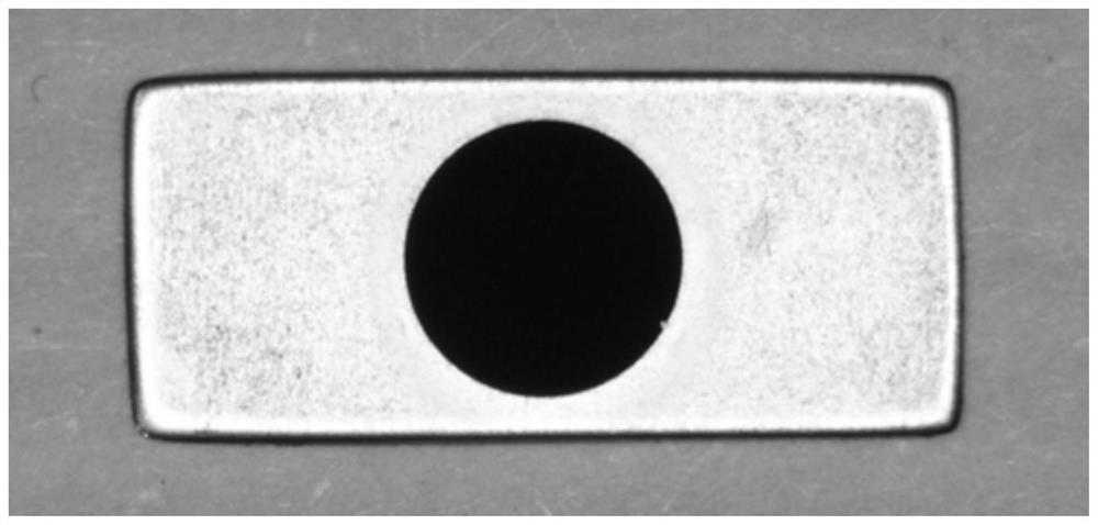
[0038] Such as figure 1 Shown, carry out the method for directly growing circular 2.5mm diameter carbon nanotube field emission cathode film on nickel-containing metal substrate in this CVD reaction device, comprise the following steps:
[0039] (1) Carry out chemical and ultrasonic cleaning to the nickel-containing metal base, and the nickel-containing metal base of the present embodiment is stainless steel;
[0040] (2) Carry out anodization treatment to nickel-containing metal substrate, select acidic solution, nickel-containing metal substrate is positive electrode, select corrosion-resistant conductor (Pt) as negative electrode, add a fixed voltage of 1V between the two electrodes for a certain period of time <10 minutes, Chemical and ultrasonic cleaning of nickel-containing metal substrates after anodizing;
[0041] (3) The pre-designed and processed 2.5mm circular mask is placed in the center of the substrate, and the substrate and the mask are placed in a physical vap...
Embodiment 2
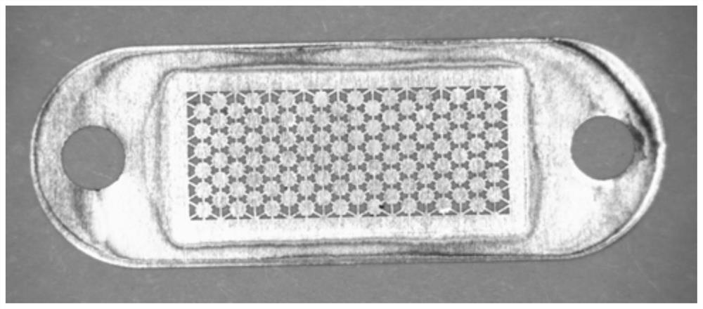
[0045] Such as figure 1 As shown, the method for directly growing the CNT field emission electron source of the array carbon nanotube field emission cathode film and the counter grid on the nickel-containing metal substrate in the CVD reaction device includes the following steps:
[0046] (1) Carry out chemical and ultrasonic cleaning to the nickel-containing metal substrate, and the nickel-containing metal substrate in this embodiment is Hastelloy;
[0047] (2) Pre-designed and processed rhombic array mask sheet ( Figure 3b) is covered on a rectangular (4×10mm) substrate, and the substrate and mask are placed in a physical vapor deposition coating system to deposit a 1 micron metal zirconium film. After the deposition, take out the substrate and remove the mask;
[0048] (3) CNT array film growth. A CVD reaction device is set, and the chemical vapor phase reaction growth of the carbon nanotube is performed on the nickel-containing metal substrate deposited with the zircon...
PUM
 Abstract
Description
Claims
Application Information


