Detection-level micro-channel plate with large size and small opening area ratio and preparation method thereof
A technology of microchannel plate and opening area, which is applied in the manufacture of luminescent cathode, secondary emitter electrode, electrode device of multiple dynodes, etc. It can solve problems such as difficult to control the effective preparation of microchannel plate
- Summary
- Abstract
- Description
- Claims
- Application Information
AI Technical Summary
Problems solved by technology
Method used
Image
Examples
preparation example Construction
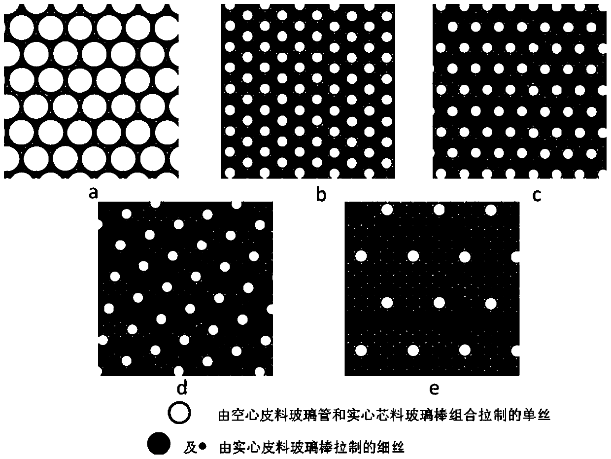
[0040] In the specific preparation process, the ratio of the mixed glass filaments to the leather glass filaments is determined based on the final opening area ratio of the microchannel plate to be realized and the ratio of the outer diameter to the inner diameter of the hollow leather glass tube used. Preferably, the ratio of the mixed glass filaments made of hollow leather glass tubes and core glass rods to the glass filaments made of solid leather glass rods is 1: (2-15).
[0041] Preferably, it also includes evaporating a magnesium oxide film layer with secondary electron emission capability on the non-channel position of the input surface on the input surface of the prepared microchannel plate by means of thermal evaporation. Preferably, the thickness of the film layer is 10nm to 30nm, so that when the non-channel position on the input surface is hit by electrons, secondary electrons will be generated, and the secondary electrons can enter the microchannel plate channel ag...
specific Embodiment 1
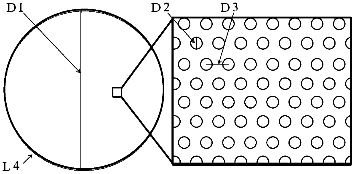
[0044] An appearance diameter size D1 is 50mm, the effective detection diameter is 45mm, the ratio of the hole spacing D3 of the microchannel plate to the channel aperture D2 is 1.5, the opening area ratio is 40%, and the non-channel position of the input surface is coated with oxide film with a thickness range of 10nm. The microchannel plate with magnesium film layer has passed the test, and its detection rate can reach 91%. It is subjected to 6 half-sine wave shocks in the parallel and vertical directions, with a peak acceleration of 1600g and no damage under the condition of a duration of 0.3ms±0.03ms. The dark current density is 5.1×10⁻¹²A / cm2.
[0045] Its production method is:
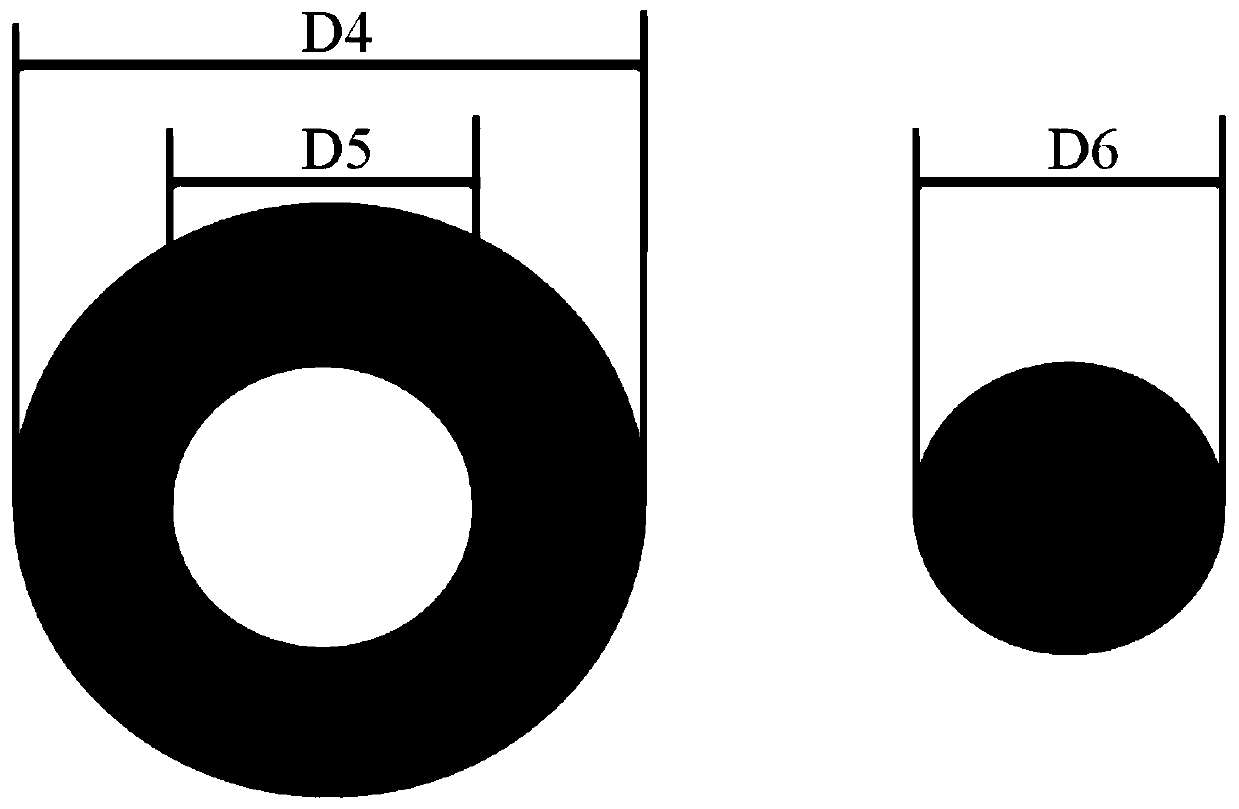
[0046] Production method 1: Select a hollow leather glass tube with an outer diameter of D4 of 31.6mm and an inner diameter of D5 of 20mm (D4: D5 = 1.58), and cooperate with a solid core material glass tube with a diameter of D6 of 20mm to pull the monofilament, arrange the wire, It is processed...
specific Embodiment 2
[0049] An appearance diameter size D1 is 81mm, the effective detection diameter is 75mm, the ratio of the hole spacing D3 of the microchannel plate to the channel aperture D2 is 2, the opening area ratio is 22.55%, and the non-channel position of the input surface is coated with oxide film with a thickness range of 15nm. The microchannel plate with magnesium film layer has passed the test, and its detection rate can reach 67%. It is subjected to 6 half-sine wave shocks in the parallel and vertical directions, with a peak acceleration of 1600g and no damage under the condition of a duration of 0.3ms±0.03ms. The dark current density is 3.2×10 -12 A / cm 2 .
[0050] Its production method is:
[0051] Production method 1: Select a hollow leather glass tube with an outer diameter of D4 of 37.8mm and an inner diameter of D5 of 18mm (D4: D5 = 2.1), and use a solid core material glass tube with a diameter of D6 of 18mm to pull the monofilament, arrange the wire, It is processed by m...
PUM
| Property | Measurement | Unit |
|---|---|---|
| Thickness | aaaaa | aaaaa |
| Dark current density | aaaaa | aaaaa |
| Outer diameter | aaaaa | aaaaa |
Abstract
Description
Claims
Application Information
 - R&D
- Intellectual Property
- Life Sciences
- Materials
- Tech Scout
- Unparalleled Data Quality
- Higher Quality Content
- 60% Fewer Hallucinations
Browse by: Latest US Patents, China's latest patents, Technical Efficacy Thesaurus, Application Domain, Technology Topic, Popular Technical Reports.
© 2025 PatSnap. All rights reserved.Legal|Privacy policy|Modern Slavery Act Transparency Statement|Sitemap|About US| Contact US: help@patsnap.com


