Array substrate and manufacturing method thereof

A technology of an array substrate and a manufacturing method, applied in the field of panels, can solve the problems of a large area occupied by a driving circuit, reducing the size of a frame of a display panel and a pixel size, etc., and achieve the effect of reducing the size of the occupied area, reducing the size of the frame, the size of the pixel, and reducing the size of the capacitor

Inactive Publication Date: 2020-05-08
FUJIAN HUAJIACAI CO LTD
View PDF4 Cites 1 Cited by
  • Summary
  • Abstract
  • Description
  • Claims
  • Application Information

AI Technical Summary

Problems solved by technology

[0004] GOA technology can make the product thinner, with higher resolution, better stability and vibration resistance, but in order to make the driving circuit have better voltage stabilization effect in the array substrate, it is usually necessary to set a larger capacity capacitor, which will As a result, the occupied area of ​​the driving circuit is large, and the frame size and pixel size of the display panel cannot be further reduced.

Method used


Image

  • Array substrate and manufacturing method thereof
  • Array substrate and manufacturing method thereof
  • Array substrate and manufacturing method thereof

Examples


Embodiment 1

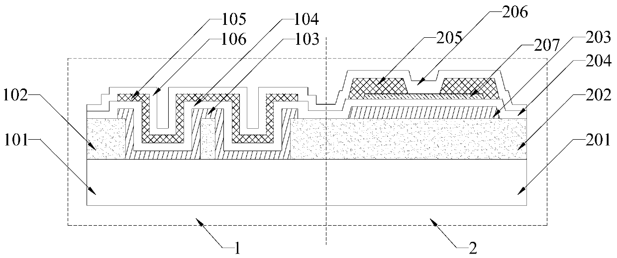
[0056] Please refer to figure 1 , Embodiment 1 of the present invention is:

[0057] An array substrate, comprising a capacitive region structure 1, the capacitive region structure 1 comprising a first substrate 101 and a first buffer layer 102;

[0058] The first buffer layer 102 is provided with two via holes, the two via holes are filled with the first gate metal layer 103, and the first gate metal layer 103 is far away from the first substrate. A first gate insulating layer 104 , a first source metal layer 105 and a first passivation layer 106 are sequentially stacked on one side of the 101 .

[0059] It also includes a TFT regional structure 2, the TFT regional structure 2 includes a second substrate 201, on the surface of the second substrate 201, a second buffer layer 202, a second gate metal layer 203, a second gate An electrode insulating layer 204, an active layer 207, a second source metal layer 205, and a second passivation layer 206, the second gate insulating l...

Embodiment 2

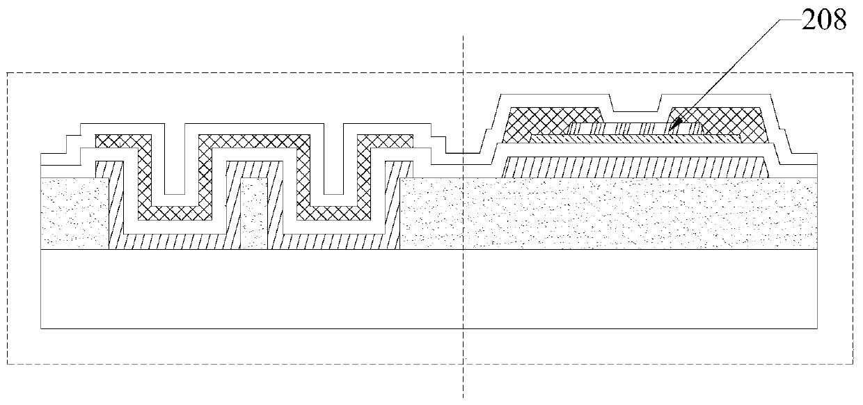
[0064] Please refer to figure 2 , the second embodiment of the present invention is:

[0065] The difference between Embodiment 2 and Embodiment 1 is that: the TFT region structure 2 further includes a second etch barrier layer 208, and the second etch barrier layer 208 is disposed on the second source metal layer 205 and the active layer 207 In between, the second etch barrier layer 208 is in contact with the second source metal layer 205 , the active layer 207 and the second passivation layer 206 respectively.

Embodiment 3

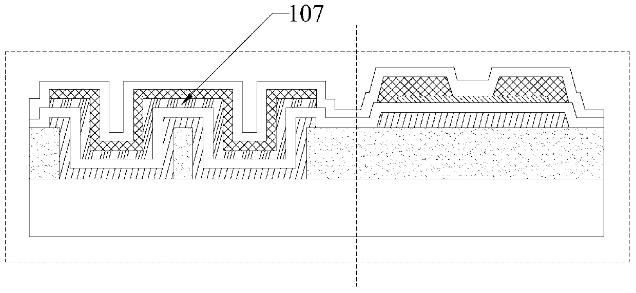
[0066] Please refer to image 3 , Embodiment three of the present invention is:

[0067] The difference between the third embodiment and the first embodiment is that the capacitive region structure 1 further includes a first etch barrier layer 107, and the first etch barrier layer 107 is disposed on the first gate insulating layer 104 and the first source metal The layers 105 are in contact with the first gate insulating layer 104 and the first source metal layer 105 respectively.


PUM


Abstract

The invention relates to the technical field of panels, and particularly relates to an array substrate and a manufacturing method thereof. More than two via holes are formed in a first buffer layer, the via holes are filled with a first gate metal layer, and a first gate insulating layer, a first source metal layer and a first passivation layer are sequentially stacked on the side surface, which is away from the first substrate, of the first gate metal layer. Due to the effect of the via holes, the first gate metal layer, the first gate insulating layer, the first source metal layer and the first passivation layer are combined to form a capacitor of a three-dimensional gate-shaped structure. Compared with an existing flat plate type capacitor, the occupied area of a capacitor area structure can be effectively reduced, the capacitor size can be further reduced under the condition that the same capacitor capacity is kept, and then the frame size and the pixel size of the display panel can be further reduced.

Description

technical field [0001] The present invention relates to the technical field of panels, in particular to an array substrate and a manufacturing method thereof. Background technique [0002] With the development of active matrix organic light emitting diode display (Active-matrix organic light emitting diode, referred to as AMOLED) and high-performance active matrix liquid crystal display (Active Matrix Liquid Crystal Display, referred to as AMLCD), in order to obtain high resolution and high frame rate display, so how to design and fabricate a high-performance and small-sized array substrate structure has become an increasingly research topic that needs to be tackled. [0003] GOA technology (GOA: Gate Driver IC on Array) is a new type of panel development in recent years. It directly etches the driving signal IC on the panel, eliminating the cost of Gate Driver IC and binding the IC to the panel. More importantly, because the Gate Driver IC is integrated with the display pa...

Claims


Application Information

Patent Timeline
Patent Type & Authority Applications(China)
IPC IPC(8): H01L27/12H01L21/77H01L27/32G02F1/1362
CPCH01L27/1255H01L27/1259H01L21/77G02F1/1362G02F1/136213H10K59/12
Inventor 陈宇怀黄志杰苏智昱
Owner FUJIAN HUAJIACAI CO LTD
Why Eureka
Try Eureka