Single-particle reinforced device structure of silicon carbide MOS and preparation method thereof

A single-event reinforcement, MOS device technology, used in semiconductor devices, electrical components, circuits, etc., can solve problems such as single-event burnout, parasitic transistor conduction burnout, etc., to improve electric field distribution, enhance short-circuit characteristics, and optimize turn-off performance. Effect

Pending Publication Date: 2020-05-08
BEIJING UNIV OF TECH +1
View PDF3 Cites 4 Cited by
  • Summary
  • Abstract
  • Description
  • Claims
  • Application Information

AI Technical Summary

Problems solved by technology

[0005] The present invention mainly aims at improving the problem that the traditional double-channel MOSFET device is prone to single-event burn-out in the space working environment, and the problem of burn-out caused by the conduction of the parasitic transistor during high-power operation

Method used


Image

  • Single-particle reinforced device structure of silicon carbide MOS and preparation method thereof
  • Single-particle reinforced device structure of silicon carbide MOS and preparation method thereof
  • Single-particle reinforced device structure of silicon carbide MOS and preparation method thereof

Examples


Embodiment Construction

[0028] Embodiments of the present invention are described below through specific examples, and those skilled in the art can easily understand other advantages and effects of the present invention from the content disclosed in this specification. The present invention can also be implemented or applied through other different specific implementation modes, and various modifications or changes can be made to the details in this specification based on different viewpoints and applications without departing from the spirit of the present invention.

[0029] The present invention will be further described below by embodiment and accompanying drawing

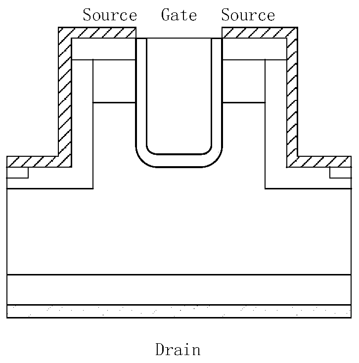
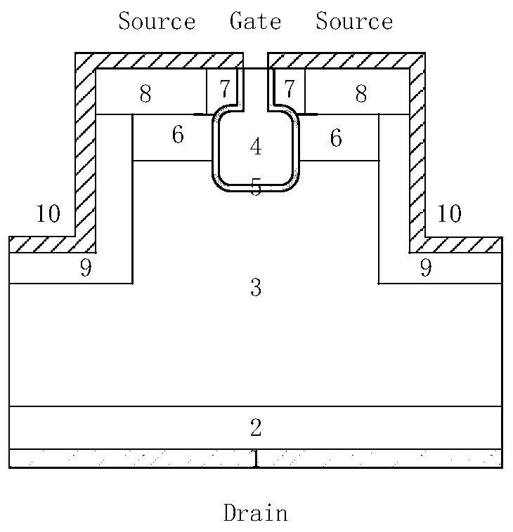
[0030] The structure of the 1200V silicon carbide power MOS device with the single-particle reinforced inverted hammer type trench gate structure of the present invention is shown in Figure 1(b), specifically including:

[0031] The drain metal 1 under the substrate 2 is located on the N-type drift region 3 on the substrate, and its d...


PUM

PropertyMeasurementUnit
Thicknessaaaaaaaaaa
Widthaaaaaaaaaa
Widthaaaaaaaaaa

Abstract

The invention relates to a single-particle reinforced device structure of a silicon carbide MOS and a preparation method of the single-particle reinforced device structure, and belongs to the technical field of semiconductor devices. According to the invention, on the basis of a double-channel MOS (DT-MOS) device, the invention provides an inverted hammer type trench gate structure and an implementation method thereof, so the latch-up effect of a parasitic NPN transistor can be inhibited, the single event burnout threshold voltage of the silicon carbide MOSFET is improved, the technical problem that the single event burnout resistance of the existing silicon carbide MOSFET technology is low is effectively solved, and the short-circuit capability and the avalanche capability of the device can also be improved. The method can be applied to design and manufacturing of devices working in high-energy charged particle environments such as spacecrafts and nuclear power stations, and the reliability and safety of an equipment system are effectively improved.

Description

Technical field: [0001] The invention relates to a single-particle-reinforced device structure and a preparation method thereof, in particular to an inverted hammer-type groove-gate structure double-channel MOS device and a preparation method thereof, belonging to the technical field of semiconductor power devices. This device is suitable for the space working environment where high-energy charged particles exist, and can improve the anti-single-event burnout ability, anti-short-circuit current ability and turn-off performance of the power MOSFET in the space working environment. Background technique: [0002] With the continuous development of aerospace technology, especially in extreme environments and working conditions such as high-power power supply systems in space, high-temperature electric propulsion processing units, and space probes, the demand for high-power high-temperature resistant devices has become increasingly obvious. [0003] Compared with the commonly use...

Claims


Application Information

Patent Timeline
IPC IPC(8): H01L29/06H01L29/423H01L29/78
CPCH01L29/0603H01L29/0615H01L29/0684H01L29/4236H01L29/78Y02B70/10
Inventor 贾云鹏赵富杰周新田赵元富胡冬青吴郁
Owner BEIJING UNIV OF TECH
Why Eureka
Try Eureka