Schottky diode and preparation method thereof

A technology of Schottky diodes and anodes, which is applied in semiconductor/solid-state device manufacturing, electrical components, circuits, etc., and can solve problems such as low on-resistance, low breakdown voltage and conduction characteristics, and high breakdown

Pending Publication Date: 2020-05-08
THE 13TH RES INST OF CHINA ELECTRONICS TECH GRP CORP
View PDF9 Cites 4 Cited by
  • Summary
  • Abstract
  • Description
  • Claims
  • Application Information

AI Technical Summary

Problems solved by technology

[0003] Wide bandgap gallium oxide Schottky diodes have the advantages of high breakdown and low on-resistance. Currently, by increasing Ga 2 o 3 The device performance of Schottky diodes has been continuously improved

Method used


Image

  • Schottky diode and preparation method thereof
  • Schottky diode and preparation method thereof
  • Schottky diode and preparation method thereof

Examples


Embodiment Construction

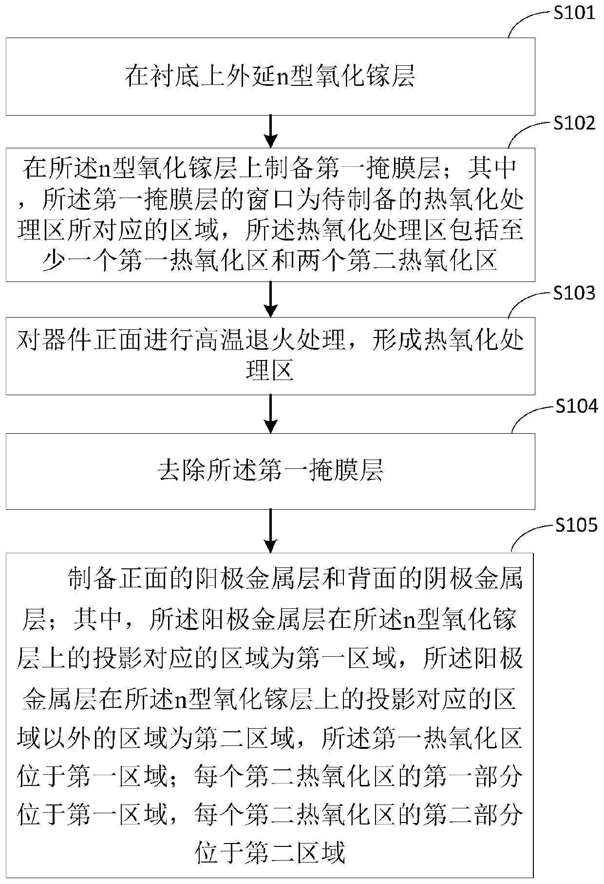
[0050] In order to make the object, technical solution and advantages of the present invention more clear, the present invention will be further described in detail below with reference to the accompanying drawings and in combination with the embodiments. It should be understood that the specific embodiments described here are only used to explain the present invention, not to limit the present invention.

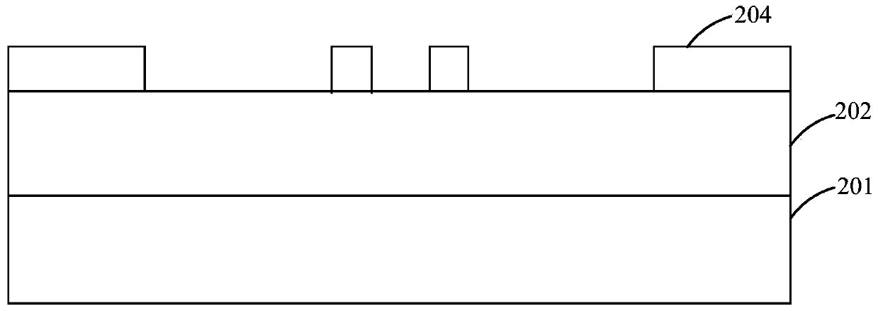
[0051] figure 1 It is a schematic flow chart of the preparation method of the Schottky diode provided by the embodiment of the present invention, refer to figure 1 , the preparation method of the Schottky diode may include:

[0052] Step S101, epitaxially growing an n-type gallium oxide layer on the substrate.

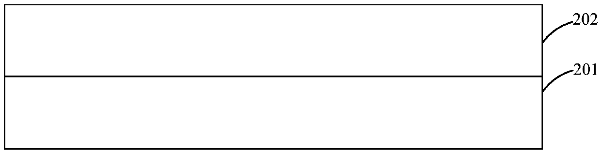
[0053] In the embodiment of the present invention, refer to figure 2 , the substrate 201 is an n-type heavily doped gallium oxide substrate. The n-type gallium oxide layer 202 is a lightly doped gallium oxide layer realized by doping Si or Sn, and the thickness o...


PUM


Abstract

The invention relates to the field of semiconductors, and particularly relates to a Schottky diode and a preparation method thereof. The method comprises the steps of extending an n-type gallium oxidelayer on a substrate; preparing a first mask layer on the n-type gallium oxide layer, wherein a window of the first mask layer is an area corresponding to a thermal oxidation treatment area to be prepared, and the thermal oxidation treatment area comprises at least one first thermal oxidation area and two second thermal oxidation areas; performing first high-temperature annealing treatment on thefront surface of the device to form a thermal oxidation treatment region; removing the first mask layer; preparing an anode metal layer on the front surface and a cathode metal layer on the back surface, the first thermal oxidation region is located below the anode metal, and each second thermal oxidation region is partially located below the anode metal. According to the method, the terminal structure can be formed through thermal oxidation, and the electric fields below the anode metal and in the edge region are reduced, so that anode reverse electric leakage is reduced, and breakdown and conduction characteristics are improved.

Description

technical field [0001] The invention relates to the field of semiconductors, in particular to a Schottky diode and a preparation method thereof. Background technique [0002] With the application of semiconductor devices in more and more technical fields, traditional silicon-based and other narrow-bandgap semiconductor diodes have encountered many challenges. Among them, the breakdown voltage is difficult to meet the growing demand, which has become one of the key factors affecting the further improvement of device performance. one. Gallium oxide (Ga 2 o 3 ) Compared with the third-generation semiconductor materials represented by SiC and GaN, it has a wider band gap, and the breakdown field strength is equivalent to more than 20 times that of Si, and more than 2 times that of SiC and GaN. In theory, When manufacturing diode devices with the same withstand voltage, the on-resistance of the device can be reduced to 1 / 10 of SiC, 1 / 3 of GaN, GaN 2 o 3 The Baliga figure of ...

Claims


Application Information

Patent Timeline
IPC IPC(8): H01L29/872H01L21/329H01L29/06
CPCH01L29/66143H01L29/872H01L29/0607Y02P70/50
Inventor 王元刚吕元杰冯志红刘红宇宋旭波周幸叶谭鑫梁士雄韩婷婷
Owner THE 13TH RES INST OF CHINA ELECTRONICS TECH GRP CORP
Why Eureka
Try Eureka