Waveguide structure integrated photon number resolution superconducting single-photon detector and preparation method thereof

A single-photon detector and integrated waveguide technology, which is applied in photometry, semiconductor devices, and superconductor parts using electric radiation detectors, can solve problems such as low detection speed and long recovery time, and achieve photon number resolution and The effect of high-speed probing application requirements

Pending Publication Date: 2020-05-08
NANJING UNIV
View PDF3 Cites 5 Cited by
  • Summary
  • Abstract
  • Description
  • Claims
  • Application Information

AI Technical Summary

Problems solved by technology

However, TES is a temperature-sensitive detector, which has di

Method used


Image

  • Waveguide structure integrated photon number resolution superconducting single-photon detector and preparation method thereof
  • Waveguide structure integrated photon number resolution superconducting single-photon detector and preparation method thereof
  • Waveguide structure integrated photon number resolution superconducting single-photon detector and preparation method thereof

Examples


Embodiment Construction

[0025] The present invention will be further explained below in conjunction with the accompanying drawings and specific embodiments.

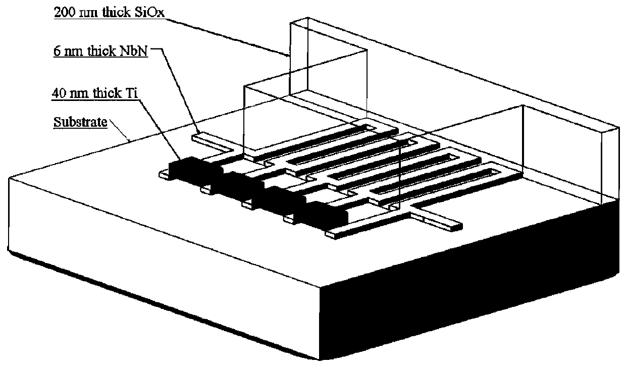
[0026] Such as figure 1 As shown, the photon detection part of the detector is a meandering nanowire structure, which is composed of 4 units connected in series. Each cell consists of a NbN meandering nanowire connected in parallel with a Ti resistor, and all resistors have the same resistance value. Each meandering nanowire has a total length of 120 μm, a width of 60 nm, and a nanowire spacing of 40 nm. The SiOx dielectric layer acts as a waveguide covering the entire nanometer region and extending outwards for transmitting incident photons.

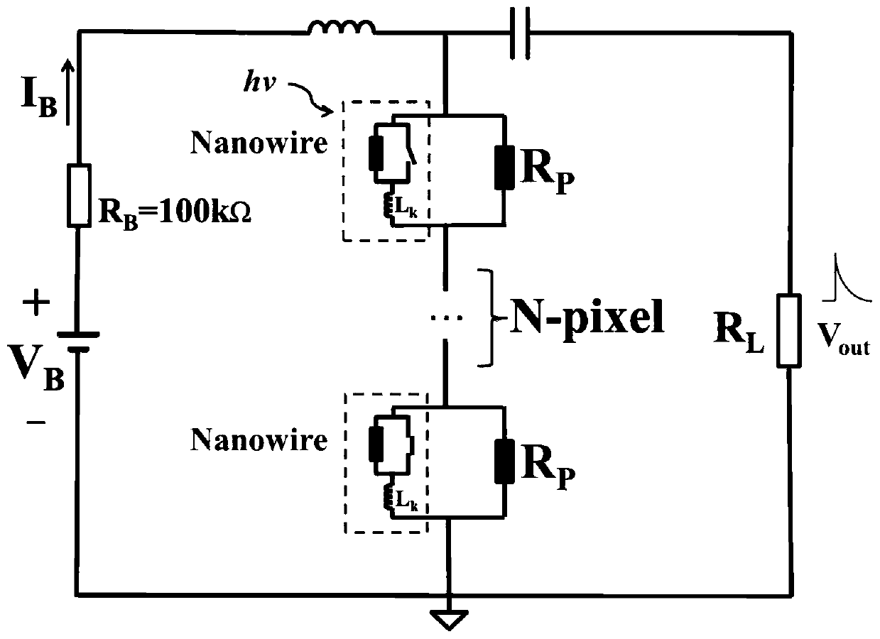
[0027] Such as figure 2 As shown, the bias current IB slightly lower than the critical current needs to be provided to the nanowires during work. Since the nanowires are in series structure, one power supply can provide the same bias to all units, and all the nanowires are in the superconducting stat...


PUM


Abstract

The invention discloses a waveguide structure integrated photon number resolution superconducting single-photon detector, and the detector comprises a substrate and a SiOx waveguide structure; a superconducting nanowire single photon detection array formed by connecting a plurality of units in series is arranged between the substrate and the SiOx waveguide, and each unit is formed by connecting aresistor and a nanowire in parallel. According to the invention, extremely weak photons transmitted by the waveguide can be detected at a high speed, the number of the detected photons can be distinguished, and the detector has important application in the field of quantum optical chips. A preparation method provided by the invention comprises the following steps: 1, carrying out magnetron sputtering on a niobium nitride superconducting film on a magnesium fluoride substrate; 2, performing photoetching and stripping to prepare an electrode; 3, preparing a nanowire pattern by electron beam lithography, and obtaining a niobium nitride nanowire array by reactive ion etching; 4, photoetching a resistor pattern, and preparing a parallel resistor; 5, preparing a waveguide pattern by electron beam lithography, and carrying out plasma enhanced chemical vapor deposition to deposit the SiOx waveguide. The preparation process disclosed by the invention is simple in steps and higher in yield.

Description

technical field [0001] The invention belongs to the technical field of superconducting single photon detection, in particular to an integrated waveguide structure photon number resolution superconducting single photon detector and a preparation method thereof. Background technique [0002] Quantum optical integrated circuits are mainly composed of single-photon sources, passive optical components and single-photon detectors. They are the core technologies in quantum communication and quantum information processing, and also form the basis of linear optical quantum computing and all-optical quantum gates. The use of waveguide structures to couple photons to single-photon detectors is beneficial to the on-chip integration of quantum optical circuits, thereby simplifying circuit complexity and measurement. Currently, only edge-transition sensors (TES) and superconducting single-photon detectors (SSPD) use waveguides. structure. However, TES is a temperature-sensitive detector,...

Claims


Application Information

Patent Timeline
IPC IPC(8): H01L39/10H01L31/09H01L31/18H01L31/0352G01J1/42
CPCH01L31/09H01L31/035227H01L31/18G01J1/42H10N60/84Y02P70/50
Inventor 张蜡宝王力波陶旭何广龙李飞燕贾小氢康琳陈健吴培亨
Owner NANJING UNIV
Why Eureka
Try Eureka