Preparation method of Cs<n>FA<1-n>PbX<3> perovskite thin film
A csnfa1-npbx3, perovskite technology, applied in semiconductor/solid-state device manufacturing, final product manufacturing, sustainable manufacturing/processing, etc., can solve the problem of difficult to obtain pure equality, achieve low cost, reduce production facilities requirements, Good film forming effect
- Summary
- Abstract
- Description
- Claims
- Application Information
AI Technical Summary
Problems solved by technology
Method used
Image

Examples
Embodiment 1
[0039] This embodiment relates to a kind of cesium iodide (CsI), iodoformamidine (FAI), lead iodide (PbI) 2 ) and dimethylamine hydroiodide (DMAI) were dissolved in DMF and then spin-coated to prepare pure phase Cs 0.5 FA 0.5 PB 3 A method for a perovskite thin film, the method comprising the steps of:
[0040] 1) 0.091g CsI, 0.060g FAI, 0.323g PbI 2 and 0.121g DMAI were dissolved in 1mL DMF to obtain precursor solution A; in the above solution, CsI, FAI, PbI 2 , The molar ratio of DMAI is 0.5:0.5:1:1;
[0041] 2) The precursor solution A obtained above was spin-coated on the FTO glass at 3000rpm for 30s, and annealed at 210°C for 5min to obtain a perovskite film.
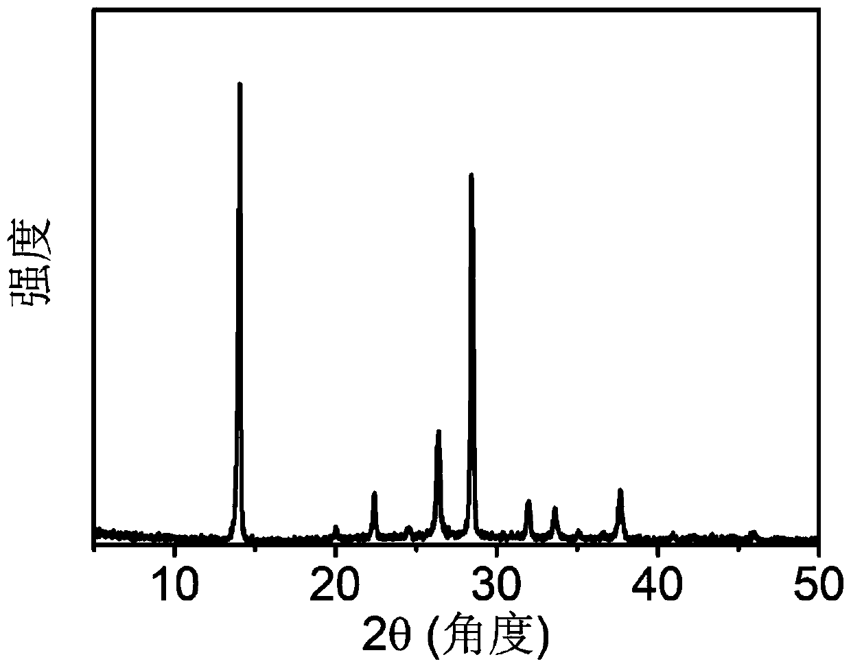
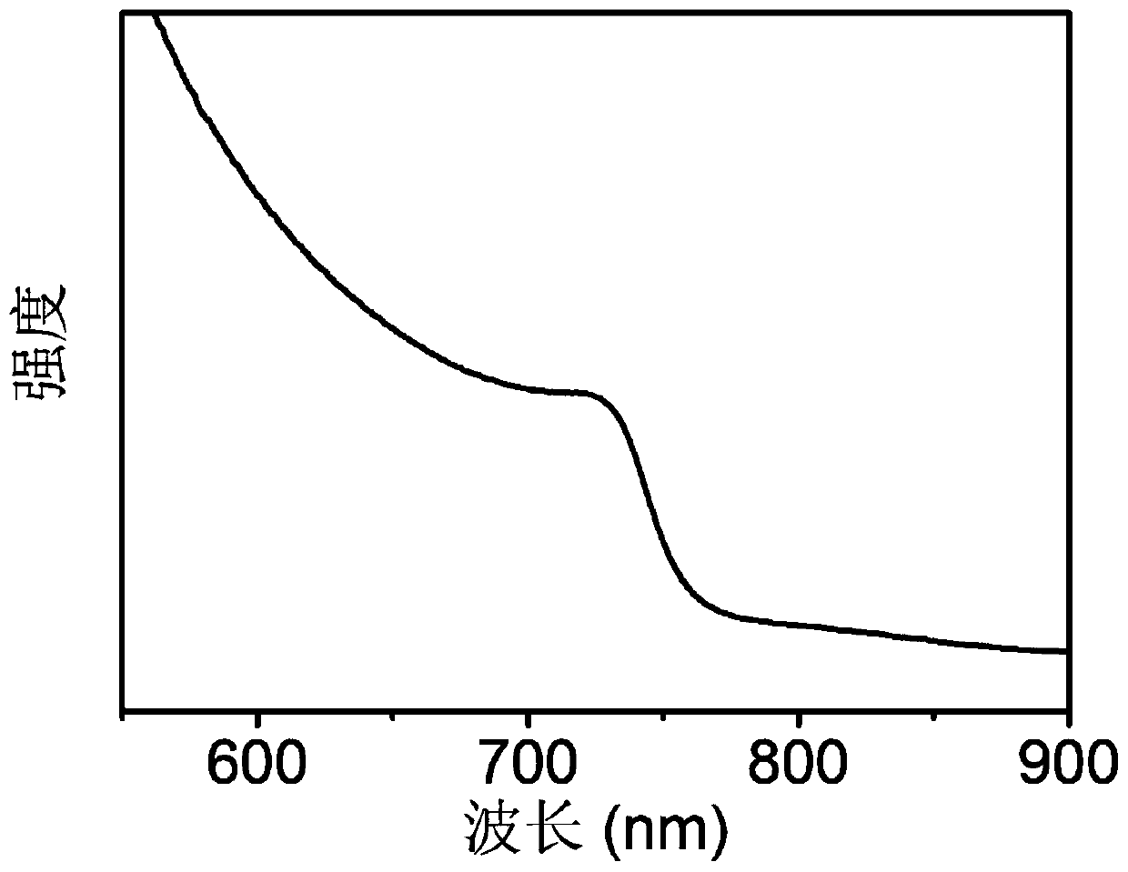
[0042] figure 1 It is the X-ray diffraction pattern of Example 1, no phase separation is found from the pattern, which proves that the Cs of pure phase has been successfully prepared 0.5 FA 0.5 PB 3 perovskite thin film. figure 2 It is the ultraviolet-visible absorption spectrum diagram of Example 1, it ...
Embodiment 2
[0044] Present embodiment method is the same as embodiment 1, and difference is that CsI, FAI, PbI in step 1) 2 , The molar ratio of DMAI is 0.9:0.1:1:1.
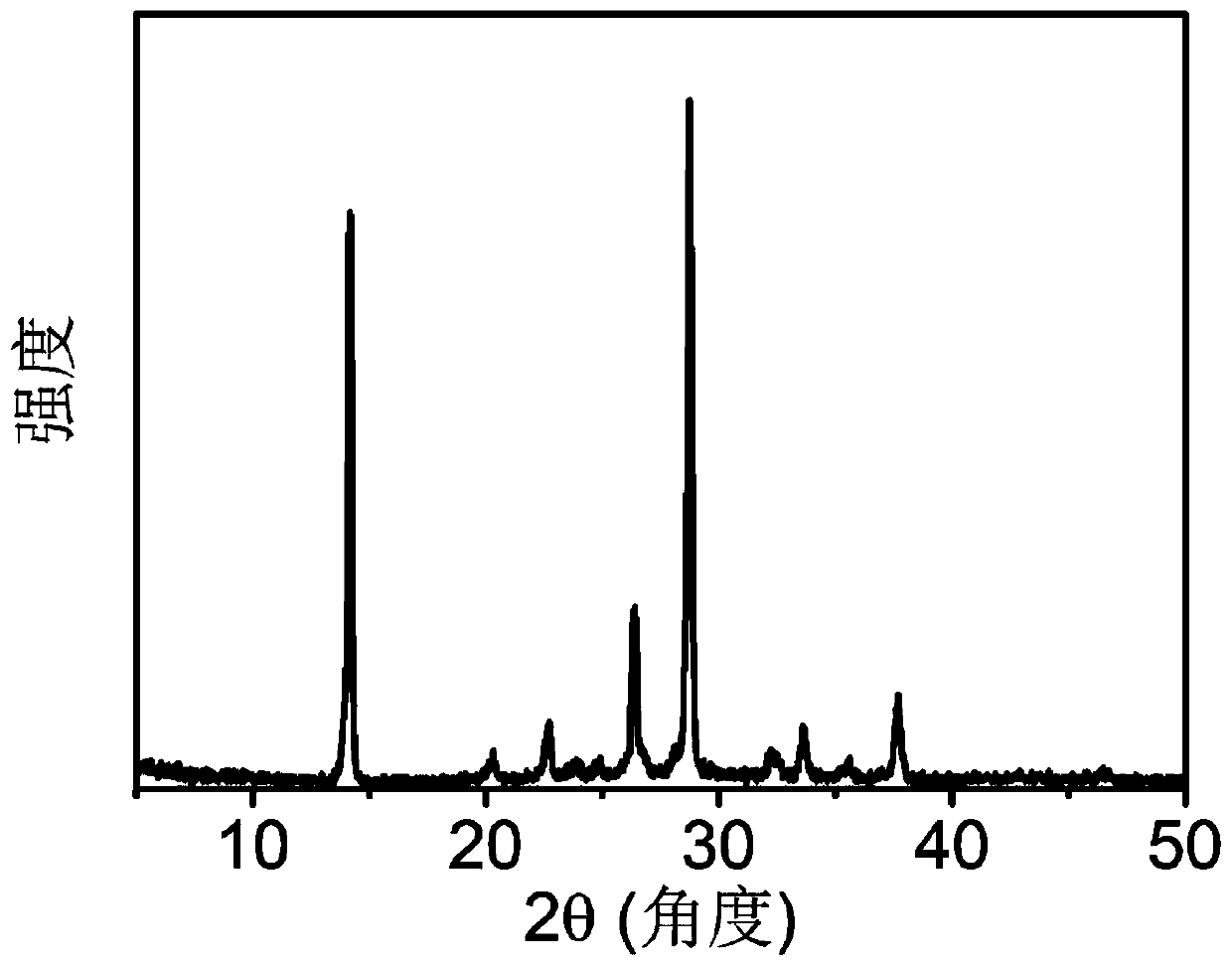
[0045] image 3 Be the X-ray diffraction pattern of embodiment 2, do not find phase separation from the pattern, show that obtained the Cs of pure phase 0.9 FA 0.1 PB 3 perovskite thin film. Figure 4 It is the ultraviolet-visible absorption spectrum diagram of Example 2, it can be seen that the characteristic absorption of perovskite appears at 742nm. The obtained perovskite film has a band gap of 1.67eV.
Embodiment 3
[0047] Present embodiment method is the same as embodiment 1, and difference is that CsI, FAI, PbI in step 1) 2 , The molar ratio of DMAI is 0.3:0.7:1:1.
[0048] Figure 5 Be the X-ray diffraction pattern of embodiment 3, do not find phase separation from the pattern, show that obtained the Cs of pure phase 0.3 FA 0.7 PB 3 perovskite thin film. The obtained perovskite film has a band gap of 1.58eV.
PUM
| Property | Measurement | Unit |
|---|---|---|
| Bandgap | aaaaa | aaaaa |
| Bandgap | aaaaa | aaaaa |
| Bandgap | aaaaa | aaaaa |
Abstract
Description
Claims
Application Information
 - R&D
- Intellectual Property
- Life Sciences
- Materials
- Tech Scout
- Unparalleled Data Quality
- Higher Quality Content
- 60% Fewer Hallucinations
Browse by: Latest US Patents, China's latest patents, Technical Efficacy Thesaurus, Application Domain, Technology Topic, Popular Technical Reports.
© 2025 PatSnap. All rights reserved.Legal|Privacy policy|Modern Slavery Act Transparency Statement|Sitemap|About US| Contact US: help@patsnap.com