
Logic circuit design method

A logic circuit and design method technology, applied in logic circuits, logic circuits using specific components, logic circuits with logic functions, etc., can solve problems such as large current attenuation, logic circuit performance, noise margin degradation, and current attenuation

Active Publication Date: 2020-05-08
HANGZHOU WEIMING XINKE TECH CO LTD +1
View PDF9 Cites 2 Cited by
  • Summary
  • Abstract
  • Description
  • Claims
  • Application Information

AI Technical Summary

Problems solved by technology

[0003] However, the nonlinear turn-on characteristics of silicon-based TFETs lead to serious attenuation of current when they are connected in series. Once TFET devices are used in standard logic unit circuits (such as multi-input NAND gates, NOR gates, etc.), the series branch is too small. Currents severely degrade logic circuit performance, noise margin, etc.
Therefore, in order to reduce the power consumption of chip integrated circuits by using the ultra-steep sub-threshold slope and ultra-low off-state current characteristics of TFETs, it is necessary to overcome the shortcomings of excessive current attenuation when they are connected in series.

Method used


Image

  • Logic circuit design method
  • Logic circuit design method
  • Logic circuit design method

Examples


Embodiment Construction

[0039] In order to make the purpose, technical solution and advantages of the present application clearer, the present application will be further described below in conjunction with the accompanying drawings and specific embodiments. It should be understood that the specific embodiments described here are only used to explain the present application, not to limit the present application. Based on the embodiments in this application, all other embodiments obtained by persons of ordinary skill in the art without making creative efforts belong to the scope of protection of this application.

[0040] Those skilled in the art can understand that, unless otherwise defined, all terms (including technical terms and scientific terms) used herein have the same meanings as commonly understood by those of ordinary skill in the art to which this application belongs. It should also be understood that terms, such as those defined in commonly used dictionaries, should be understood to have m...


PUM


Abstract

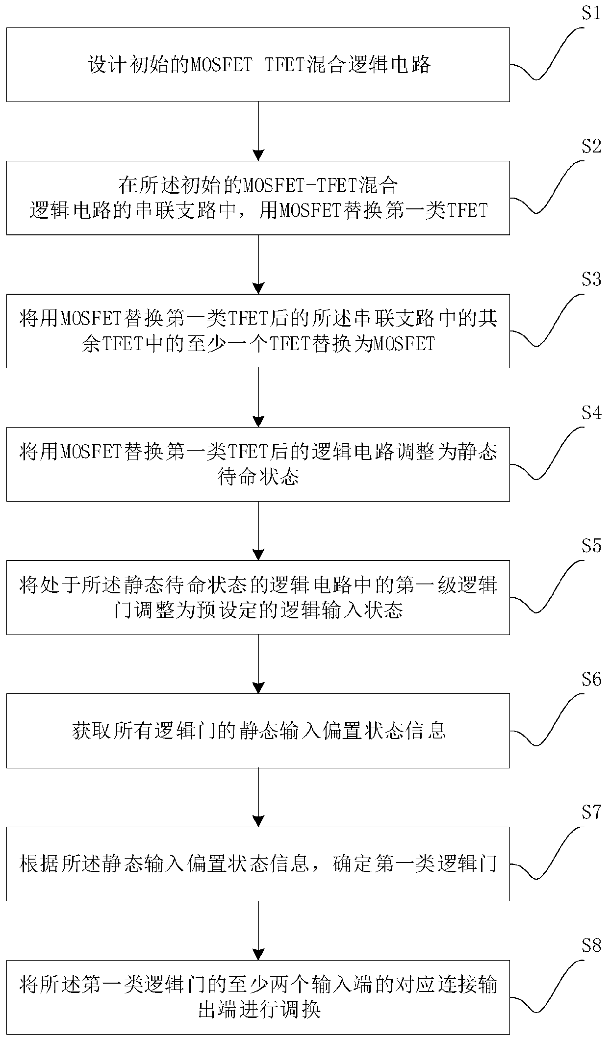
The invention discloses a logic circuit design method and apparatus, and a storage medium. The method comprises the steps of designing and generating an initial MOSFET-TFET hybrid logic circuit, wherein the MOSFET-TFET hybrid logic circuit comprises a plurality of logic gates; in a series branch of the initial MOSFET-TFET hybrid logic circuit, replacing a first type of TFET with an MOSFET, whereinthe first type of TFETs are directly grounded or connected with a power supply and are not directly connected with the output end of the logic gate. According to the logic circuit design method disclosed in the invention, by replacing the first type of TFET in the series branch of the initial logic circuit with the MOSFET, the defect of overlarge current attenuation caused by the TFET in the series branch is overcome, and the first type of TFET is a TFET which is directly grounded or powered and is not directly connected with the output end of the logic gate.

Description

technical field [0001] The present application relates to the technical field of integrated circuits, in particular to a method for designing logic circuits. Background technique [0002] In the past few decades, with the continuous shrinking of the size of semiconductor devices, the performance of integrated circuit chips has been continuously improved, but the power consumption of the system has gradually increased. This problem has slowed down the further reduction of device sizes. Since the subthreshold slope has a theoretical limit of 60mV / dec at room temperature, it is difficult for traditional MOSFET devices to continuously reduce the operating voltage V DD to reduce power consumption. MOSFET is Metal-Oxide Semiconductor Field-Effect Transistor, referred to as Metal-Oxide-Semiconductor Field-Effect Transistor (MOSFET). In order to adapt to the future development trend of integrated circuits, research on new ultra-low power devices has attracted widespread attention....

Claims


Application Information

Patent Timeline
IPC IPC(8): H03K19/00H03K19/094H03K19/0944H03K19/08H03K19/20H03K19/21
CPCH03K19/0013H03K19/09425H03K19/0944H03K19/08H03K19/20H03K19/215G06F30/398G06F2119/06G06F30/327Y02D10/00
Inventor 叶乐王志轩黄芊芊王阳元黄如
Owner HANGZHOU WEIMING XINKE TECH CO LTD
Learn More