Chip structure
A chip structure, chip technology, applied in the direction of instruments, using re-radiation, antenna arrays that are powered separately, etc., can solve the problems of silicon-based technology performance limitation noise figure, increased chip size, low integrity, etc.
- Summary
- Abstract
- Description
- Claims
- Application Information
AI Technical Summary
Problems solved by technology
Method used
Image


Examples
Embodiment Construction
[0014] In radar applications, digital circuits and RF circuits need to be used together. To perform multi-channel digital and RF procedures on a single chip, silicone-based structures are often used. However, the overall performance of the single chip structure is limited due to the limited RF performance of the silicone-based structure. Accordingly, the present invention provides chip architectures that implement digital and RF applications.
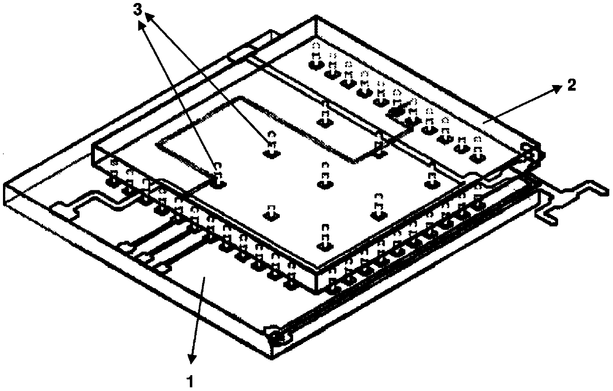
[0015] figure 1 A perspective view of a chip structure of the present invention is shown. The chip structure comprises at least one gallium-based (eg gallium arsenide-GaAs, gallium nitride-GaN, etc.) first layer (1) for RF applications; at least one gallium-based (eg gallium arsenide-GaAs, gallium nitride Gallium-GaN, etc.) second layer (2) placed on said first layer (1) to perform digital applications; at least two copper layers between the first layer (1) and the second layer (2) The base pillar (3) provides electrical connection...
PUM
 Abstract
Description
Claims
Application Information
 - R&D
- Intellectual Property
- Life Sciences
- Materials
- Tech Scout
- Unparalleled Data Quality
- Higher Quality Content
- 60% Fewer Hallucinations
Browse by: Latest US Patents, China's latest patents, Technical Efficacy Thesaurus, Application Domain, Technology Topic, Popular Technical Reports.
© 2025 PatSnap. All rights reserved.Legal|Privacy policy|Modern Slavery Act Transparency Statement|Sitemap|About US| Contact US: help@patsnap.com