Low roll-off quasi-two-dimensional perovskite light-emitting diode and its preparation method

A technology of light-emitting diodes and perovskites, which is applied in semiconductor/solid-state device manufacturing, semiconductor devices, electrical components, etc., can solve problems such as poor film quality, many film grain boundaries, and device efficiency roll-off, and achieve low cost, Effects of suppressing non-radiative recombination and suppressing efficiency roll-off

Active Publication Date: 2021-11-05
SHANGHAI UNIV
View PDF2 Cites 0 Cited by
  • Summary
  • Abstract
  • Description
  • Claims
  • Application Information

AI Technical Summary

Problems solved by technology

However, compared with the traditional three-dimensional perovskite, quasi-two-dimensional perovskite has more grain boundaries in the film due to the reduced grain size, and the quality of the film is deteriorated, and the device efficiency rolls off seriously under high voltage, which is a common problem of perovskite LEDs. question

Method used


Image

  • Low roll-off quasi-two-dimensional perovskite light-emitting diode and its preparation method
  • Low roll-off quasi-two-dimensional perovskite light-emitting diode and its preparation method
  • Low roll-off quasi-two-dimensional perovskite light-emitting diode and its preparation method

Examples


Embodiment 1

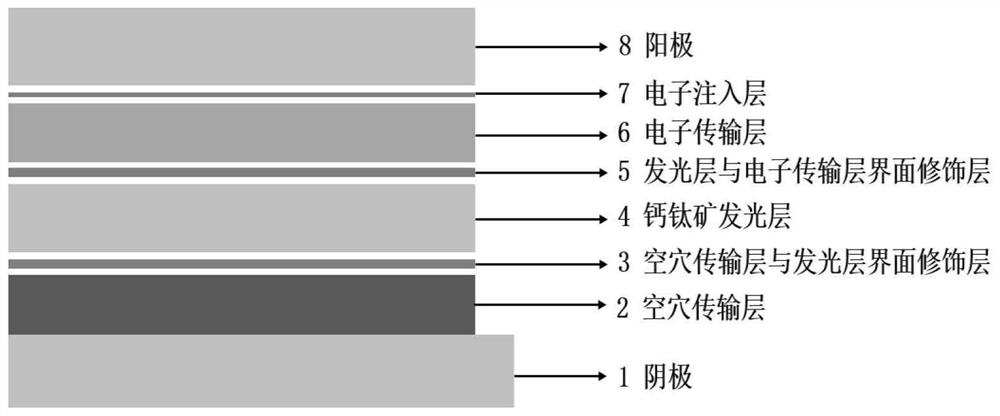
[0050] In this example, see figure 1, a low-roll-off quasi-two-dimensional perovskite light-emitting diode, in which an anode 1, a hole transport layer 2, an interface modification layer 3 between the hole transport layer and the light-emitting layer, a perovskite light-emitting layer 4, and a light-emitting layer are sequentially arranged from bottom to top Layer and electron transport interface modification layer 5, electron transport layer 6, electron injection layer 7, cathode 8;

[0051] The thickness of the anode 1 is 150nm, and the gate 1 adopts an ITO conductive glass film; the thickness of the hole transport layer 2 is 50nm, and the hole transport layer 2 is made of PEDOT:PSS; the hole The thickness of the interface modification layer 3 between the transmission layer and the light-emitting layer is 10nm, and cesium carbonate (Cs 2 CO 3 ) is made; the thickness of the perovskite light-emitting layer 4 is 100nm; the thickness of the light-emitting layer and the electr...

Embodiment 2

[0075] This embodiment is basically the same as Embodiment 1, especially in that:

[0076] In this example, see figure 1 , a low-roll-off quasi-two-dimensional perovskite light-emitting diode, in which an anode 1, a hole transport layer 2, an interface modification layer 3 between the hole transport layer and the light-emitting layer, a perovskite light-emitting layer 4, and a light-emitting layer are sequentially arranged from bottom to top Layer and electron transport interface modification layer 5, electron transport layer 6, electron injection layer 7, cathode 8;

[0077] The thickness of the anode 1 is 100nm, and the gate 1 adopts an ITO conductive glass film; the thickness of the hole transport layer 2 is 40nm, and the hole transport layer 2 is made of PEDOT:PSS; the hole The thickness of the interface modification layer 3 between the transmission layer and the light-emitting layer is 1nm, and cesium carbonate (Cs 2 CO 3 ) is made; the thickness of the perovskite ligh...


PUM

PropertyMeasurementUnit
thicknessaaaaaaaaaa
thicknessaaaaaaaaaa
thicknessaaaaaaaaaa

Abstract

The invention discloses a low-roll-off quasi-two-dimensional perovskite light-emitting diode and a preparation method thereof. A cathode, a hole transport layer, an interface modification layer between the hole transport layer and the light-emitting layer, and a perovskite light-emitting diode are sequentially arranged from bottom to top. Layer, light-emitting layer and electron transport interface modification layer, electron transport layer, electron injection layer, anode. The present invention not only reduces the hole injection barrier between the hole layer and the light-emitting layer by modifying the interface between the hole transport layer and the perovskite light-emitting layer, but also improves the hole injection efficiency, and can block the impact of the hole layer on the perovskite. The quenching of the mineral layer improves the luminous efficiency of the perovskite layer. The invention also modifies the interface between the perovskite light-emitting layer and the electron transport layer, which can not only passivate the defect states on the surface of the perovskite, but also improve the film quality of the light-emitting layer and inhibit non-radiative recombination, thereby further improving the luminous efficiency of the device.

Description

technical field [0001] The invention relates to a perovskite light-emitting diode and a preparation method thereof, in particular to a quasi-two-dimensional perovskite light-emitting diode and a preparation method thereof, which are applied in the technical field of semiconductor material preparation technology. Background technique [0002] As a new and efficient semiconductor material, perovskite has many superior optical properties. Compared with the commercialized organic light-emitting diode (OLED), it has a narrow half-width, a spectrum that can cover the full wavelength range, and is soluble Therefore, it has become a current research hotspot. In recent years, perovskites have shown considerable application value in solar cells, LED lighting, photodetectors, lasers, and flat panel displays. However, most current LEDs face efficiency roll-off at high voltages, which limits the commercialization of perovskites to a certain extent. Therefore, the high-voltage stability...

Claims


Application Information

Patent Timeline
Patent Type & Authority Patents(China)
IPC IPC(8): H01L51/50H01L51/56
CPCH10K71/15H10K71/12H10K50/16H10K50/15
Inventor 杨绪勇张婷
Owner SHANGHAI UNIV
Why Eureka
Try Eureka